Image processing device, image processing method, and program
An image processing device and image data technology, applied in image data processing, image enhancement, image communication, etc., can solve problems such as inability to correctly detect defective blocks, inability to accurately calculate difference values, etc.
- Summary
- Abstract
- Description
- Claims
- Application Information
AI Technical Summary
Problems solved by technology
Method used
Image


Examples
Embodiment approach 1
[0051] 〔Structure of the camera system〕
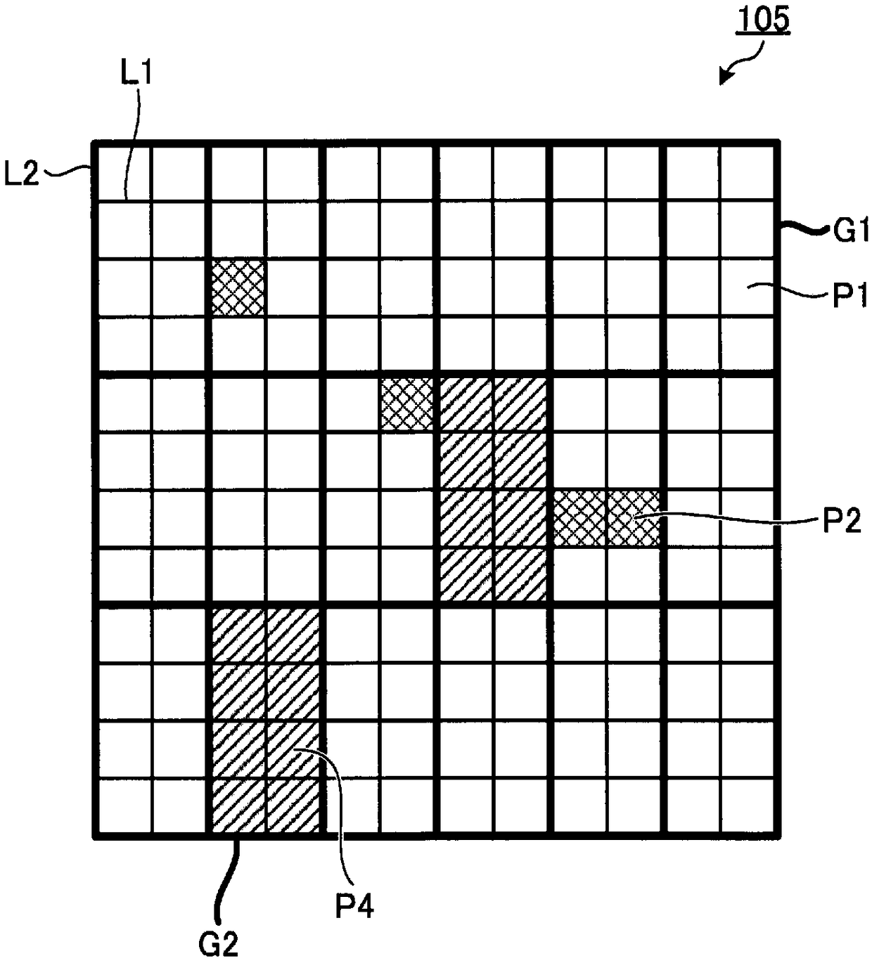
[0052] figure 1 It is a block diagram schematically showing the configuration of the imaging system according to Embodiment 1 of the present invention. figure 1 The camera system 1 shown has a camera device 10 , an image processing device 20 , and a display device 30 .
[0053] [Structure of camera device]
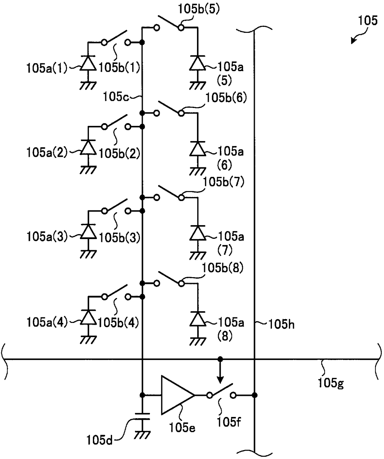
[0054] First, the configuration of the imaging device 10 will be described. Such as figure 1 As shown, the imaging device 10 has an optical system 101, an aperture 102, a shutter 103, a driver 104, an imaging element 105, an analog processing unit 106, an A / D conversion unit 107, an operation unit 108, a memory interface unit 109, a recording medium 110, an A volatile memory 111, a nonvolatile memory 112, a bus 113, an imaging control unit 114, and a first external interface unit 115.
[0055] The optical system 101 is configured using a plurality of lenses. The optical system 101 is configured using, for example, a focus len...
Embodiment approach 2
[0120] Next, Embodiment 2 of the present invention will be described. This second embodiment has the same configuration as the imaging system 1 of the above-mentioned first embodiment, but the offset calculation process is different. Next, the offset calculation processing performed by the offset calculation unit according to Embodiment 2 will be described. In addition, the same code|symbol is attached|subjected to the same structure as the imaging system 1 of Embodiment 1 mentioned above, and description is abbreviate|omitted.
[0121] [Outline of offset calculation processing]
[0122] Figure 8 It is a flowchart showing the outline of the offset calculation process according to the second embodiment. In addition, in Embodiment 2, the offset calculation unit 222 and the offset calculation unit 231 respectively perform the same processing, so only the offset calculation processing when the offset calculation unit 222 executes it will be described.
[0123] Such as Figure ...
Embodiment approach 3
[0130] Next, Embodiment 3 of the present invention will be described. The imaging system of Embodiment 3 has the same configuration as the imaging system 1 of Embodiment 1 described above, but the offset calculation process is different. Next, the offset calculation processing performed by the offset calculation unit according to Embodiment 3 will be described. In addition, the same code|symbol is attached|subjected to the same structure as the imaging system 1 of Embodiment 1 mentioned above, and description is abbreviate|omitted.
[0131] [Outline of offset calculation processing]
[0132] Figure 10 It is a flowchart showing the outline of the offset calculation process in the third embodiment. In addition, in Embodiment 3, the offset calculation unit 222 and the offset calculation unit 231 respectively perform the same processing, so only the offset calculation processing when the offset calculation unit 222 executes it will be described.
[0133] Such as Figure 10 A...
PUM
 Abstract
Description
Claims
Application Information
 - R&D
- Intellectual Property
- Life Sciences
- Materials
- Tech Scout
- Unparalleled Data Quality
- Higher Quality Content
- 60% Fewer Hallucinations
Browse by: Latest US Patents, China's latest patents, Technical Efficacy Thesaurus, Application Domain, Technology Topic, Popular Technical Reports.
© 2025 PatSnap. All rights reserved.Legal|Privacy policy|Modern Slavery Act Transparency Statement|Sitemap|About US| Contact US: help@patsnap.com