Packaging structure and packaging method for chip

A packaging method and chip technology, applied in the direction of semiconductor/solid-state device components, semiconductor devices, electrical components, etc., can solve the problems of poor packaging structure performance and achieve the effect of improving performance

Active Publication Date: 2018-09-28
SUZHOU TF AMD SEMICON CO LTD
View PDF7 Cites 1 Cited by
  • Summary
  • Abstract
  • Description
  • Claims
  • Application Information

AI Technical Summary

Problems solved by technology

[0003] However, the performance of the package structure formed by the existing 3D packaging process is poor

Method used


Image

  • Packaging structure and packaging method for chip
  • Packaging structure and packaging method for chip
  • Packaging structure and packaging method for chip

Examples


Embodiment Construction

[0031] As mentioned in the background, the performance of the packaging structure formed by the existing 3D packaging process is poor.

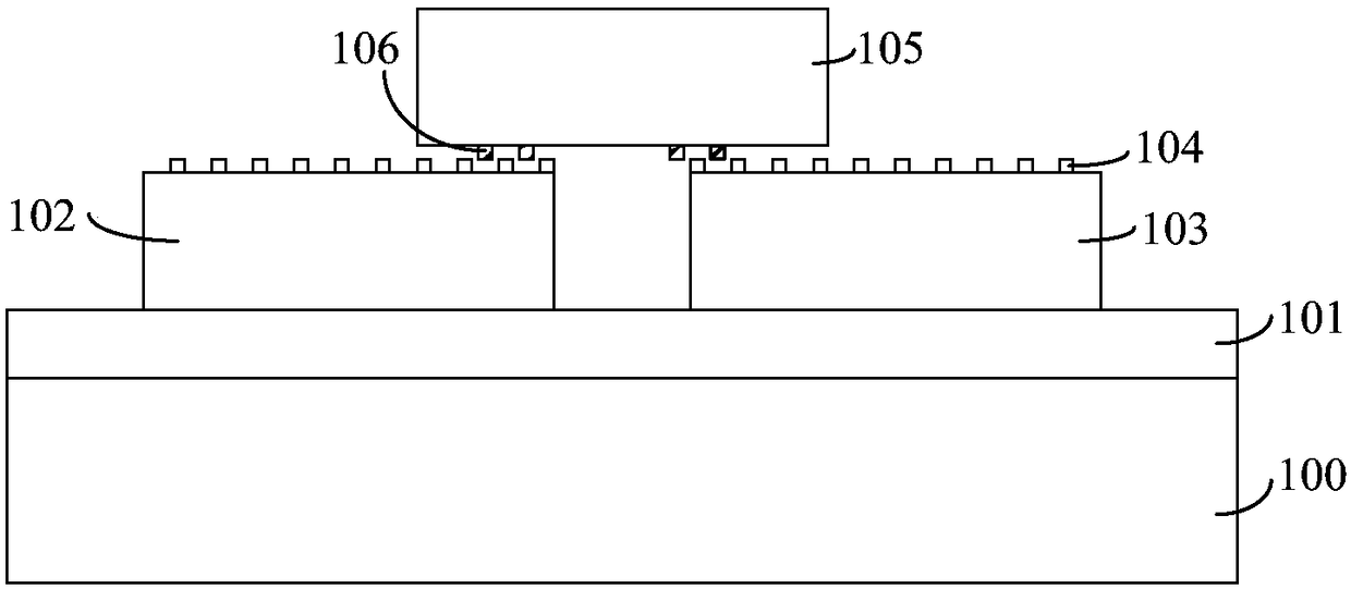
[0032] figure 1 It is a structural schematic diagram of a chip packaging structure.

[0033] Please refer to figure 1 , providing a carrier board 100, the surface of the carrier board 100 has a mounting film 101; on the surface of the mounting film 101, a first chip 102 and a second chip 103 separated from each other are mounted, and the first chip 102 and the second chip 103 are mounted on the surface of the mounting film 101. The top of the second chip 103 has a first connection column 104; a third chip 105 is provided, and the top of the third chip 105 has a second connection column 106; the third chip 105 is mounted so that the second connection column 106 is connected to the first connection column Post 104 contacts.

[0034] In the above chip packaging method, the surface of the carrier 100 has a first identification point for identi...


PUM


Abstract

The invention discloses a packaging structure and packaging method for a chip. The packaging method comprises the steps of providing a substrate, wherein the surface of the substrate is provided witha placement film; a first chip is placed on the surface of the placement film; the first chip comprises opposite first surface and second surface; and the second surface is attached to the surface ofthe placement film; providing a plurality of second chips, wherein each second chip comprises a third surface and a first region; placing the second chips on the corresponding third surfaces towards the first surface, wherein the first regions of the second chips are overlapped with one part of the first chip and salient points are arranged between the first surface and the third surfaces of the first regions; and after placing the second chips, melting the salient points and electrically connecting the second chips and the first chip. The packaging structure formed through the method is relatively good in performance.

Description

technical field [0001] The invention relates to the field of semiconductor manufacturing, in particular to a packaging structure and a forming method thereof. Background technique [0002] As the density of integrated circuit packaging continues to increase, the size of the chip continues to decrease, and the number of I / O terminals continues to increase, but more and more functions are required on the effective size of the chip. For the problems caused by packaging, 3D packaging in the Z direction can be considered. The use of 3D packaging technology can increase packaging density, improve product performance, reduce power consumption, reduce noise, and realize multi-function and miniaturization of electronic equipment. [0003] However, the performance of the packaging structure formed by the existing 3D packaging process is poor. Contents of the invention [0004] The technical problem solved by the invention is to provide a chip packaging structure and a packaging me...

Claims


Application Information

Patent Timeline
Patent Type & Authority Applications(China)
IPC IPC(8): H01L23/31H01L23/498H01L21/56
CPCH01L21/561H01L23/3121H01L23/49811H01L23/49833
Inventor 邱原陈传兴
Owner SUZHOU TF AMD SEMICON CO LTD
Why Eureka
Try Eureka