A board-level package design optimization method for integrated qfn chips
An optimization method, integrated circuit board technology, applied in design optimization/simulation, computer-aided design, CAD circuit design, etc., to achieve the effects of low processing cost and process difficulty, improved efficiency and convergence, and good engineering practicability
- Summary
- Abstract
- Description
- Claims
- Application Information
AI Technical Summary
Problems solved by technology
Method used
Image

Examples
Embodiment Construction
[0033] The present invention will be further described below in conjunction with the accompanying drawings and embodiments.
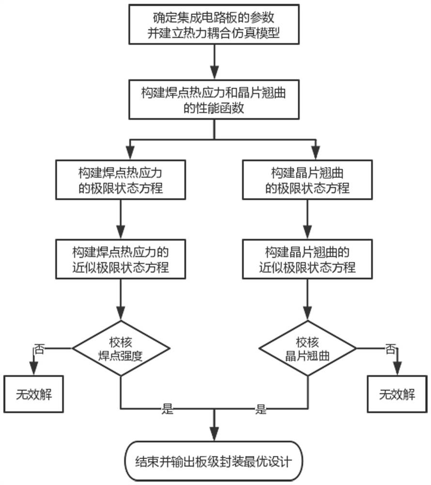
[0034] refer to figure 1 As shown, the present invention relates to a board-level packaging design optimization method for integrated QFN chips, and the steps are as follows.
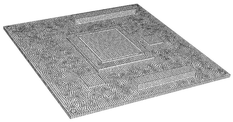
[0035] 1) Step 1, determine the parameters of the integrated circuit board and establish a thermal-mechanical coupling simulation model
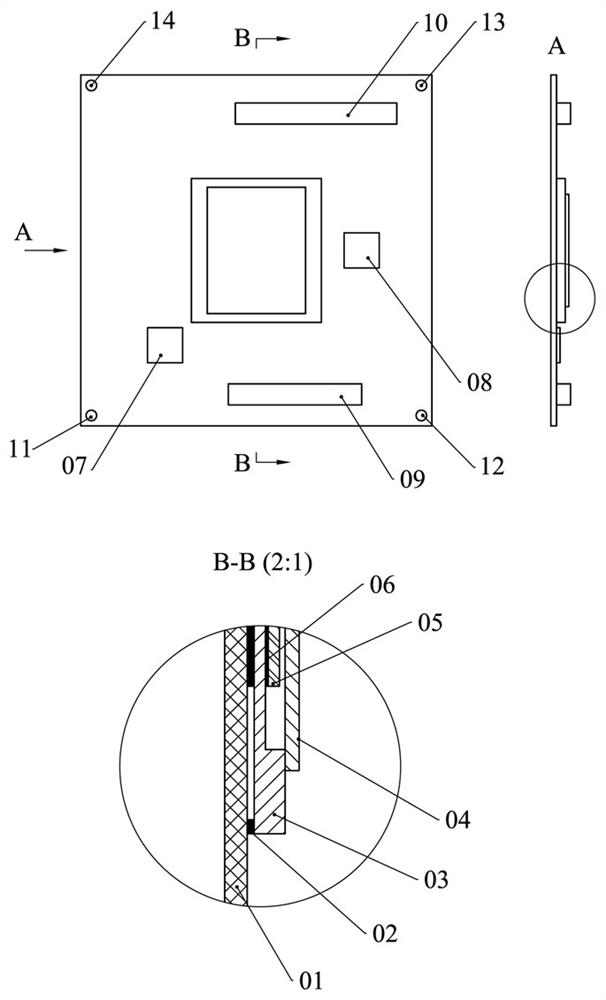
[0036] refer to figure 2 As shown, according to the existing information, determine the parameters of the integrated circuit board, including: substrate 01, QFN chip parts 02~06 and device 07~10 structural dimensions, plane coordinates, elastic modulus, Poisson's ratio, thermal expansion coefficient, Working heat consumption, as well as the plane coordinates of fixed points 11~12, and the working temperature range of the integrated circuit board [-20°C, 60°C]; the specific information is listed in Table 1 and Table 2. According to the abov...
PUM
 Abstract
Description
Claims
Application Information
 - R&D
- Intellectual Property
- Life Sciences
- Materials
- Tech Scout
- Unparalleled Data Quality
- Higher Quality Content
- 60% Fewer Hallucinations
Browse by: Latest US Patents, China's latest patents, Technical Efficacy Thesaurus, Application Domain, Technology Topic, Popular Technical Reports.
© 2025 PatSnap. All rights reserved.Legal|Privacy policy|Modern Slavery Act Transparency Statement|Sitemap|About US| Contact US: help@patsnap.com