Supercharge Your Innovation With Domain-Expert AI Agents!

A realization method of micro-LED chip interconnection

A technology of LED chips and implementation methods, applied in semiconductor devices, electrical components, circuits, etc., can solve the problems of difficult packaging process, low optical power of micron-level LEDs, poor heat dissipation, etc., to reduce process difficulty, good heat dissipation performance, Improve the effect of insulating layer materials

Active Publication Date: 2020-09-08
PEKING UNIV
View PDF10 Cites 0 Cited by
  • Summary
  • Abstract
  • Description
  • Claims
  • Application Information

AI Technical Summary

Problems solved by technology

[0004] The purpose of the present invention is to provide a method for realizing the internal interconnection structure of micro-LED chips, which solves the problems of low optical power, poor heat dissipation and difficult packaging process of micro-LEDs at present, and realizes the high-voltage and high-power performance target of GaN-based micro-LEDs

Method used


Image

  • A realization method of micro-LED chip interconnection
  • A realization method of micro-LED chip interconnection
  • A realization method of micro-LED chip interconnection

Examples


Embodiment Construction

[0020] After the sapphire substrate LED epitaxial wafer is pickled, organic cleaned, and deionized water rinsed until the surface is free of contamination and oxide layer and dried, a layer of ITO is evaporated as a current spreading layer;

[0021] Coater coating photoresist, through exposure and development, to form a number of mesa array photolithographic patterns, the pattern size is 5-200 microns;

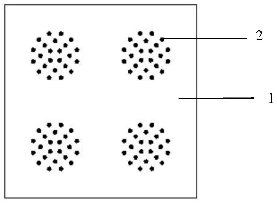
[0022] Use ICP dry etching to etch away the area not protected by the photoresist until the structural layer forms a mesa, and the mesa size is 5-200 microns, such as figure 1 shown;

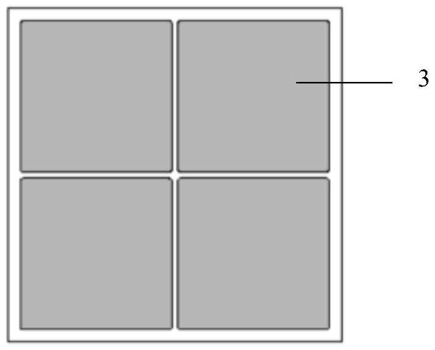
[0023] The coater coats the photoresist, and through exposure and development, the isolation area between the arrays is formed, such as figure 2 Shown with 4 LED array units isolated from each other;

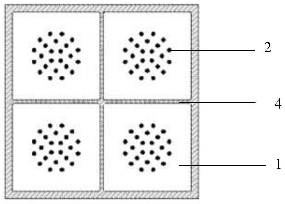
[0024] Plasma deeply etches the area not protected by the photoresist to the upper surface of the structural layer to form an array isolation region; the number and size of the isolation regio...


PUM


Abstract

The invention provides a method for realizing interconnection in micron LED chips, and belongs to the technical field of photoelectronic high-power light emitting devices. The method not only realizesthe high voltage and high power characteristics of the LED chips, but also avoids the difficulty of integrating a large number of micron-scale chips in subsequent packaging, thereby reducing requirements for the packaging equipment and technology, and being capable of greatly improving the device performance of micron LEDs. The method not only combines the excellent characteristic of great injection of the micron LEDs, but also reduces the preparation difficulty at the same time, thereby having important practical and guiding significance for the application of the micron LEDs to various emerging industries.

Description

technical field [0001] The invention relates to an optoelectronic high-power light-emitting device, in particular to a method for realizing interconnection in micron LED chips. Background technique [0002] As the LED industry matures, LED energy-saving green light sources have replaced a considerable portion of incandescent lamps, fluorescent lamps, etc., and are widely used in lighting, display, biomedical and other fields. In recent years, the excellent photoelectric characteristics of micro-LEDs have attracted the attention of many research groups, and various emerging applications based on micro-LEDs are also being researched in full swing, such as micro-flat panel display, optical interconnection, visible light communication, wearable devices, and biological detection imaging. Wait. [0003] Higher and wider applications place higher requirements on the performance of LED chips. However, due to the severe droop effect and poor heat dissipation of traditional LED chip...

Claims


Application Information

Patent Timeline
Patent Type & Authority Patents(China)
IPC IPC(8): H01L33/00H01L33/38H01L33/64
CPCH01L33/007H01L33/387H01L33/641
Inventor 陈志忠李诚诚康香宁焦飞冯玉龙詹景麟于彤军沈波
Owner PEKING UNIV
Features
  • R&D
  • Intellectual Property
  • Life Sciences
  • Materials
  • Tech Scout
  • Unparalleled Data Quality
  • Higher Quality Content
  • 60% Fewer Hallucinations
Learn More