Ultrathin EMI-resistant thin film and preparation method thereof

An ultra-thin, thin-film technology used in electrical components, magnetic/electric field shielding, etc.

Pending Publication Date: 2018-10-02
白国华
View PDF4 Cites 5 Cited by
  • Summary
  • Abstract
  • Description
  • Claims
  • Application Information

AI Technical Summary

Problems solved by technology

[0004] The purpose of the present invention is to provide a kind of ultra-thin anti-EMI film and preparation method thereof for the above-mentioned problem of existing anti-EMI material

Method used


Image

  • Ultrathin EMI-resistant thin film and preparation method thereof
  • Ultrathin EMI-resistant thin film and preparation method thereof
  • Ultrathin EMI-resistant thin film and preparation method thereof

Examples


Embodiment 1

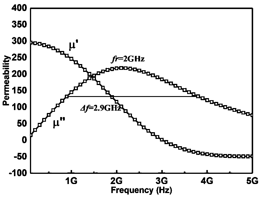
[0036] 4μm PET is used as the substrate, and a 0.05μm Ag layer is deposited on the substrate by vacuum evaporation as a metal reflective layer; (FeCo) 0.8 Al 0.2 The alloy is used as the target material, and at room temperature, the sub-layers of 0.5 μm are deposited by magnetron sputtering in the oxygen fraction of 0.02, 0.04, 0.06, 0.08, 0.10, 0.15, 0.4, 0.8, and 1.2 mtorr, in which the volume fraction of FeCo particles is determined by from 85% to 25%.

[0037] Carry out magnetic performance test on it, the magnetic permeability is 300, the cut-off frequency is 2GHz, Δf 2.9GHz.

Embodiment 2

[0039] Using 10μm copper foil as the substrate, using electroless plating to prepare a 0.1μm Ni layer on the substrate as the metal reflective layer; using Fe and SiO 2 Composite target material, using magnetron sputtering to sequentially deposit composite sublayers with Fe particle volume fractions of 95%, 90%, 80%, 70%, 60%, 50%, 40%, and 30%.

[0040] It is tested for its magnetic performance, the magnetic permeability is 240, and the cut-off frequency is 1.5GHz. Δf 1.8GHz.

Embodiment 3

[0042] Using 6μm PI as the substrate, using electron beam deposition to evaporate a 2μm Cu layer on the substrate as a metal reflective layer; using PrCo 5 and Al 2 o 3 As a composite target, a 1 μm first composite sublayer was deposited by magnetron sputtering at room temperature, where PrCo 5 Particle volume fraction is 80%; using (FeCo) 0.7 Al 0.3 Alloy as the target material, at room temperature, in 0.6mtorr oxygen concentration, magnetron sputtering deposits 0.5μm second composite sublayer, in which the volume fraction of FeCo is 68%; 0.6 Al 0.4 , at room temperature, in 0.8mtorr oxygen, magnetron sputtering deposits a 0.5μm third composite sublayer, in which the volume fraction of Fe is 48%; using Fe 0.4 Al 0.6 , at room temperature, in 1mtorr oxygen gas, magnetron sputtering deposited a 0.5μm fourth composite sublayer, in which the volume fraction of Fe was 28%;

[0043] Carry out magnetic performance test on it, the magnetic permeability is 180, the cut-off freq...


PUM

PropertyMeasurementUnit
thicknessaaaaaaaaaa
thicknessaaaaaaaaaa
absorption bandwidthaaaaaaaaaa

Abstract

The invention discloses an ultrathin EMI-resistant thin film and a preparation method thereof. The main structure of the ultrathin EMI-resistant thin film comprises substrate / metal reflection layer / composite gradient layer, wherein the ultrathin composite gradient layer is provided with a structure of which magnetic particles are dispersed in a dielectric matrix and is in gradient distribution along a thickness direction of the thin film, impedance matching is favorably achieved, and the application frequency and the EMI-resistant frequency are improved. By the ultrathin EMI-resistant thin film, the ultrathin EMI-resistant thin film with the thickness blew 12 micrometers can be prepared, the ultrathin EMI-resistant thin film can have favorable EMI-resistant performance within a frequency band above 1GHz, and miniaturization and integration of an electronic product are very facilitated.

Description

technical field [0001] The invention relates to an ultra-thin anti-EMI film and a preparation method thereof, belonging to the field of new materials and new technologies of electronic components. Background technique [0002] Electromagnetic interference (EMI) is a ubiquitous source of electromagnetic pollution. In the AC state, electronic devices will radiate electromagnetic waves to the environment, which will cause interference to surrounding electronic components or products. With the rapid development of electronic technology, the functions of electronic products are becoming more and more powerful, and the integration of devices and operating frequency are required to be higher and higher. At the same time, the equipment needs to be miniaturized, which makes the problem of EMI more and more prominent, which seriously affects the normal operation of devices. Work. There is an urgent need for anti-EMI materials with light, thin, and wide-band characteristics. Anti-EM...

Claims


Application Information

Patent Timeline
Patent Type & Authority Applications(China)
IPC IPC(8): H05K9/00
CPCH05K9/0081
Inventor 白国华
Owner 白国华
Why Eureka
Try Eureka