bias circuit

A bias circuit and bias current technology, applied in electrical components, adjusting electrical variables, instruments, etc., can solve the problems of the chip occupying a large area, the difficulty of the bias circuit, and the incompetence of cost-effectiveness, so as to maintain normal operation. Effect

Active Publication Date: 2020-04-07
RICHWAVE TECH CORP
View PDF5 Cites 0 Cited by
  • Summary
  • Abstract
  • Description
  • Claims
  • Application Information

AI Technical Summary

Problems solved by technology

However, relatively speaking, if the design of the bias circuit in the integrated circuit is carried out using the III-V process, it is very difficult to design the bias circuit by setting the operational amplifier.
Even if it can be produced, the circuit structure of this bias circuit will be very complicated, and it will occupy a large area on the chip, which is not cost-effective

Method used


Image

  • bias circuit
  • bias circuit
  • bias circuit

Examples


Embodiment Construction

[0029] Various exemplary embodiments will be described more fully hereinafter with reference to the accompanying drawings, in which some exemplary embodiments are shown. However, inventive concepts may be embodied in many different forms and should not be construed as limited to the illustrative embodiments set forth herein. Rather, these exemplary embodiments are provided so that this disclosure will be thorough and complete, and will fully convey the scope of the inventive concept to those skilled in the art. Like numerals indicate like components throughout the various figures of the specification.

[0030] The bias circuit provided by the present invention will be described below with multiple embodiments, however, the following embodiments are not intended to limit the present invention.

[0031] An embodiment of a bias circuit

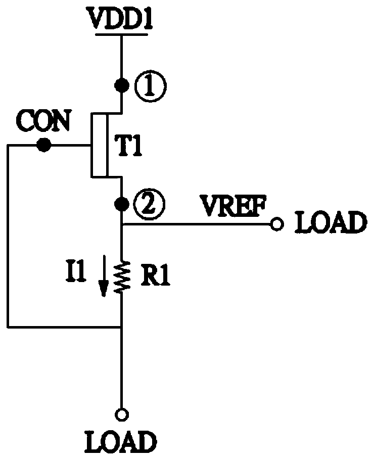
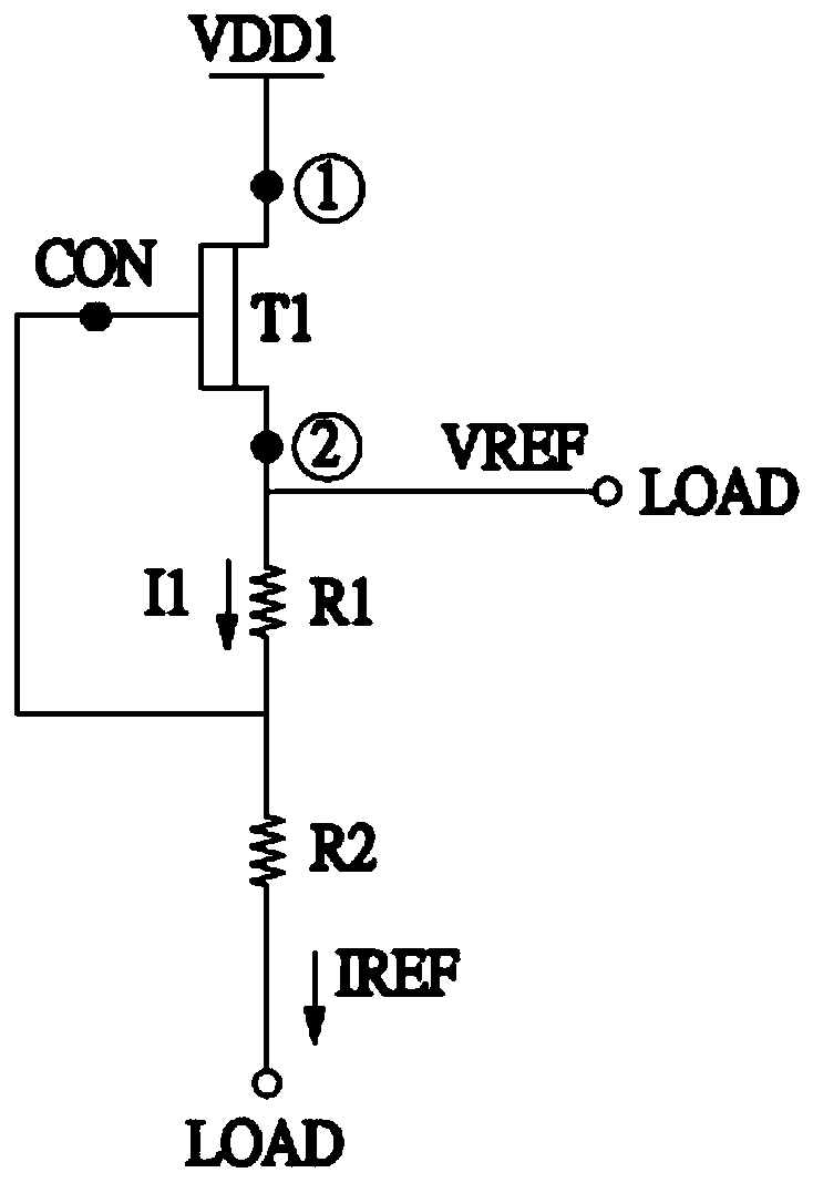
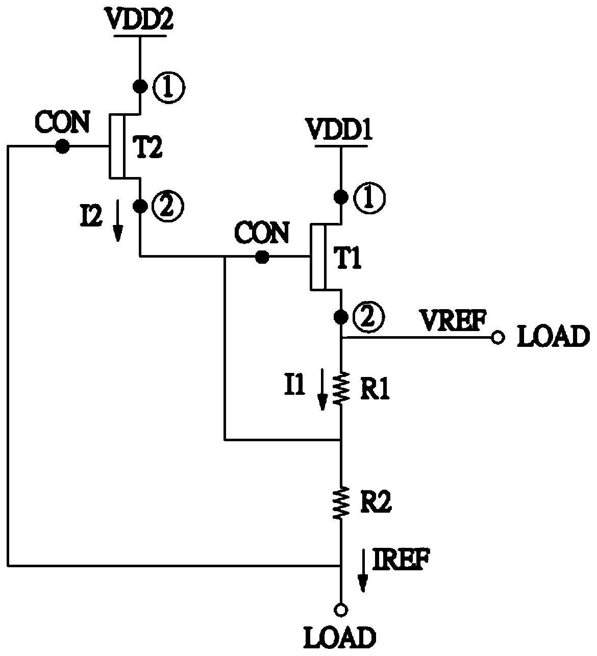
[0032] Please refer to Figure 1A and Figure 1B , Figure 1A and Figure 1B is a circuit diagram of a bias circuit according to an exemplar...


PUM


Abstract

A bias circuit includes a first transistor, a second transistor, a first resistor and a second resistor. The first end of the first transistor is coupled to a first voltage source. One end of the first resistor is coupled to the second end of the first transistor, and the other end of the first resistor is coupled to the control terminal of the first transistor. The first end of the second transistor is coupled to a second voltage source, and the second end of the second transistor is coupled to the control terminal of the first transistor. One end of the second resistor is coupled to the other end of the first resistor, and the other end of the second resistor is coupled to the control terminal of the second transistor.

Description

technical field [0001] The present invention relates to a bias circuit, in particular to a bias circuit capable of providing a stable reference voltage or bias current. Background technique [0002] As far as the design of the bias circuit in the integrated circuit is concerned, generally speaking, if the SOI (Silicon On Insulator) process or the Complementary Metal Oxide Semiconductor (CMOS) process is used, the setting of the operational amplifier will be used to set the bias voltage. The reference voltage to be generated by the voltage circuit is locked at a voltage value that meets the operating requirements of the load. This method is very easy and convenient when using SOI process or complementary metal oxide semiconductor process to design the bias circuit in the integrated circuit. intuitive. However, relatively speaking, it is very difficult to design the bias circuit by using an operational amplifier when the bias circuit in the integrated circuit is designed usin...

Claims


Application Information

Patent Timeline
Patent Type & Authority Patents(China)
IPC IPC(8): G05F1/56
CPCG05F1/561G05F3/16H03F1/223H03F1/301H03F2200/18H03F2200/21H03F2200/294H03F2200/451H01L27/0629H03F1/302H03F5/00
Inventor 陈智圣彭天云林昭毅
Owner RICHWAVE TECH CORP
Why Eureka
Try Eureka