Method of manufacturing semiconductor device

A manufacturing method, semiconductor technology, applied in semiconductor/solid-state device manufacturing, semiconductor devices, electrical components, etc.

Active Publication Date: 2018-10-09
FUJI ELECTRIC CO LTD
View PDF23 Cites 2 Cited by
  • Summary
  • Abstract
  • Description
  • Claims
  • Application Information

AI Technical Summary

Problems solved by technology

For example, it is known that an IGBT (Insulated Gate Bipolar Transistor: Insulated Gate Bipolar Transistor) and an FWD (Free Wheeling Diode: Free Wheeling Diode) connected in antiparallel to the IGBT are integrated in the same semiconductor chip. In the reverse conducting IGBT (RC-IGBT), helium (He) is irradiated while n - Type drift region formation will be the defect of lifetime controlling body

Method used


Image

  • Method of manufacturing semiconductor device
  • Method of manufacturing semiconductor device
  • Method of manufacturing semiconductor device

Examples


Embodiment approach

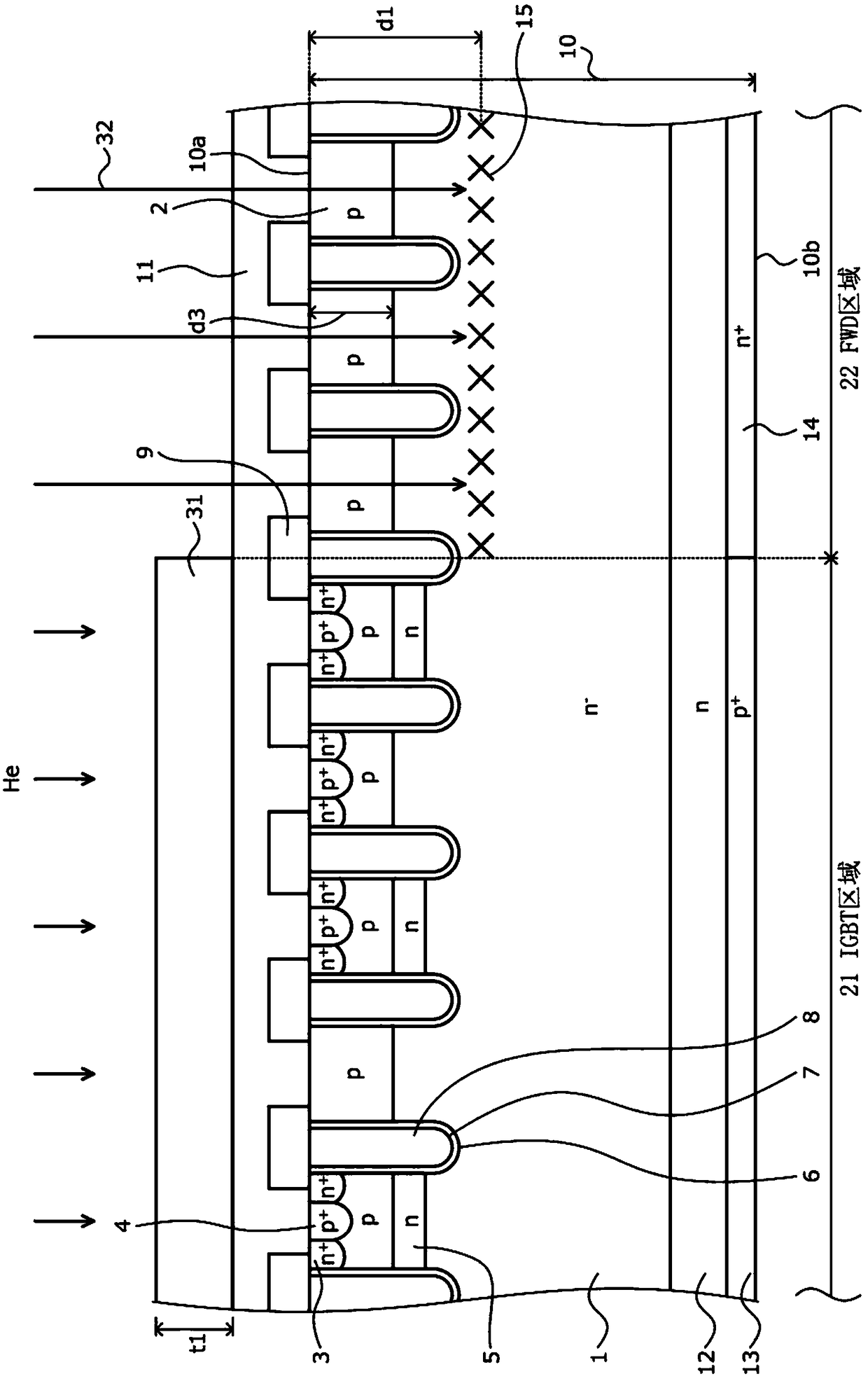
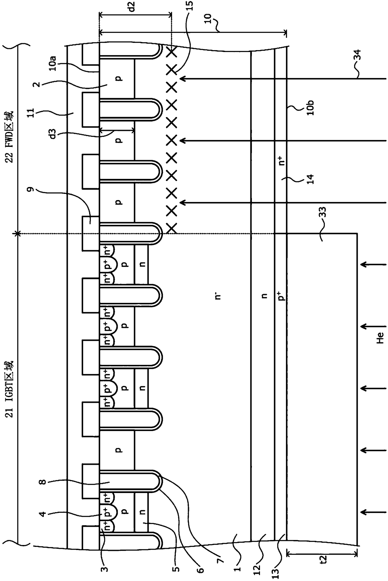
[0074] The manufacturing method of the semiconductor device according to the embodiment will be described taking, as an example, an RC-IGBT of a breakdown voltage of 1200 V class in which helium defects are introduced by irradiation of helium (He) in the FWD region. The so-called withstand voltage is a limit voltage at which a device does not malfunction and / or be destroyed. figure 1 It is a cross-sectional view showing the state during the manufacturing process of the semiconductor device according to the embodiment. figure 2 It is a cross-sectional view showing another example of the state in the manufacturing process of the semiconductor device according to the embodiment. exist figure 1 , figure 2 In , the states where helium irradiation is performed from the front side 10 a side and the back side 10 b side of the semiconductor wafer 10 are schematically shown, respectively.

[0075] The RC-IGBT is formed, for example, by integrating an IGBT having a trench gate str...


PUM

PropertyMeasurementUnit
depthaaaaaaaaaa
widthaaaaaaaaaa
thicknessaaaaaaaaaa

Abstract

The present invention provides a method for manufacturing a semiconductor device capable of avoiding reduction of design margin caused for shape collapsing of an end portion of a slushing compound pattern when a photoresist is taken as a mask. The method of manufacturing a semiconductor device, includes the steps of: providing a semiconductor wafer (10), forming a photoresist film (31) on a main surface of the semiconductor wafer, forming a first mask pattern and a second mask pattern on the photoresist film (31), selectively removing portions of the photoresist film (31) according to the first and second mask patterns, to respectively form a first opening and a second opening in the photoresist film (31), a position of the second opening differing from that of the first opening, and performing ion implantation of an impurity into the semiconductor wafer (10), using the photoresist film (31) having the first and second openings formed therein as a mask (31).

Description

technical field [0001] The present invention relates to a method of manufacturing a semiconductor device. Background technique [0002] Conventionally, a power device has been developed in which an impurity defect serving as a lifetime controller is introduced by ion implantation with a high acceleration energy, thereby improving characteristics and improving the characteristics. For example, it is known that an IGBT (Insulated Gate Bipolar Transistor: Insulated Gate Bipolar Transistor) and an FWD (Free Wheeling Diode: Free Wheeling Diode) connected in antiparallel to the IGBT are integrated in the same semiconductor chip. In the reverse conducting IGBT (RC-IGBT), helium (He) is irradiated while n - Type drift region formation will be a defect of lifetime control body. [0003] Figure 11 , Figure 12 It is a cross-sectional view showing the structure of a conventional RC-IGBT. exist Figure 11 As shown in the previous RC-IGBT, the n - Near the interface between p-type ...

Claims


Application Information

Patent Timeline
Patent Type & Authority Applications(China)
IPC IPC(8): H01L21/266H01L21/322H01L21/336
CPCH01L21/266H01L21/3221H01L29/66409H01L29/32H01L29/407H01L29/8613H01L21/26506H01L29/7397H01L29/0834H01L29/0692H01L29/66348H01L29/6609H01L21/0274H01L21/0275H01L21/027H01L21/046H01L21/0273
Inventor 儿玉奈绪子
Owner FUJI ELECTRIC CO LTD
Why Eureka
Try Eureka