Doping preparation and repair method for graphene

A repair method, graphene technology, applied in the field of graphene doping preparation and repair, can solve the problems of incomplete plane size, surface attachment impurities, low reaction temperature, etc., to achieve smooth surface, wide range of applicable substrates, doping reaction The effect of low temperature

Active Publication Date: 2018-10-16
恒力(厦门)石墨烯科技产业集团有限公司
View PDF10 Cites 10 Cited by
  • Summary
  • Abstract
  • Description
  • Claims
  • Application Information

AI Technical Summary

Problems solved by technology

The present invention prepares high-quality and large-size graphene film by CVD method, firstly ensures that the quality of graphene is intact, and then performs doping by MPCVD method, the reaction temperature is low, the applicable base materials are more extensive, and the do

Method used


Image

  • Doping preparation and repair method for graphene

Examples


Embodiment Construction

[0037] The following will clearly and completely describe the technical solutions in the embodiments of the present invention with reference to the accompanying drawings in the embodiments of the present invention. Obviously, the described embodiments are only some, not all, embodiments of the present invention.

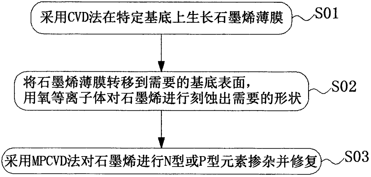
[0038] see figure 1, the present invention provides a technical solution: a graphene-doped preparation and repair method, the steps of the graphene-doped preparation and repair method are as follows:

[0039] S01: first grow a graphene film on a specific substrate by CVD;

[0040] S02: Transfer the graphene film to the required substrate surface, and use oxygen plasma to etch the graphene to obtain the desired shape;

[0041] S03: Then use the MPCVD method to do N-type or P-type element doping on the graphene and repair it.

[0042] As a preferred embodiment of the present invention, the specific substrate can be any one of copper foil, nickel foil, gold foil, tita...


PUM


Abstract

The invention belongs to the field of semiconductor preparation and discloses a doping preparation and repair method for graphene. The method comprises the following steps: a graphene film grows on aspecific substrate with a CVD method; the graphene film is transferred to the surface of a required substrate, and graphene is etched in a required shape by oxygen plasma; N-type or P-type element doping is performed on graphene with an MPCVD method, and semiconductor graphene is repaired during doping. The prepared semiconductor graphene is applicable to wider substrates, concentration of dopingelements is controllable, part of graphene defects in a semiconductor can be overcome by repairing, a semiconductor graphene film with a certain area can be formed by flaky semiconductor graphene andhas lower impedance and shorter response time.

Description

technical field [0001] The invention belongs to the technical field of semiconductor preparation, and in particular relates to a method for preparing and repairing graphene doping. Background technique [0002] Graphene is a two-dimensional material composed of a single layer of C atoms. Due to its excellent electrical and mechanical properties, graphene has become one of the candidate materials to replace silicon in the post-Moore era. However, intrinsic graphene is a zero-bandgap semiconductor or semimetal, which limits the application and development of graphene in the semiconductor field. Through lattice doping, some carbon atoms in graphene are replaced with other atoms, so that the doped graphene has the property of many electrons or holes, that is, N-type or P-type doped semiconductor graphene is obtained, and The semiconductor graphene doped by lattice has stable performance and has great prospects for industrial application. [0003] Generally, in the application ...

Claims


Application Information

Patent Timeline
IPC IPC(8): C01B32/194C01B32/186
CPCC01B32/186C01B32/194
Inventor 陈木成
Owner 恒力(厦门)石墨烯科技产业集团有限公司
Why Eureka
Try Eureka