Method for thinning sapphire wafer

A sapphire wafer and sapphire technology, applied in stone processing equipment, fine working devices, electrical components, etc., can solve problems such as heat dissipation and grounding problems of high-power devices, complex precision processing technology, and difficult machining, and achieve small deformation , fill the technical gap, and achieve the effect of complete chip structure

Active Publication Date: 2011-10-12
INST OF MICROELECTRONICS CHINESE ACAD OF SCI
View PDF4 Cites 27 Cited by
  • Summary
  • Abstract
  • Description
  • Claims
  • Application Information

AI Technical Summary

Problems solved by technology

Although the performance of aluminum gallium nitride / gallium nitride (AlGaN / GaN) HEMT power devices (high electron mobility transistors) has made great progress in recent years, especially in terms of high frequency and high power, there are still many problems that have not been resolved. The problem of heat dissipation and grounding of devices has always plagued the practical and industrialization of AlGaN / GaN HEMTs
[0005] Due to its high hardness (Mohs hardness 9.5, second only to diamond with Mohs 10.0) and high brittleness, sapphire is very difficult to machine, and chemical reactions will occur in acid-base environments. For sapphire substrates with complex circuit structures, the precision processing technology is more complicated, which is a difficult problem in current research.

Method used


Image

  • Method for thinning sapphire wafer
  • Method for thinning sapphire wafer

Examples


Embodiment Construction

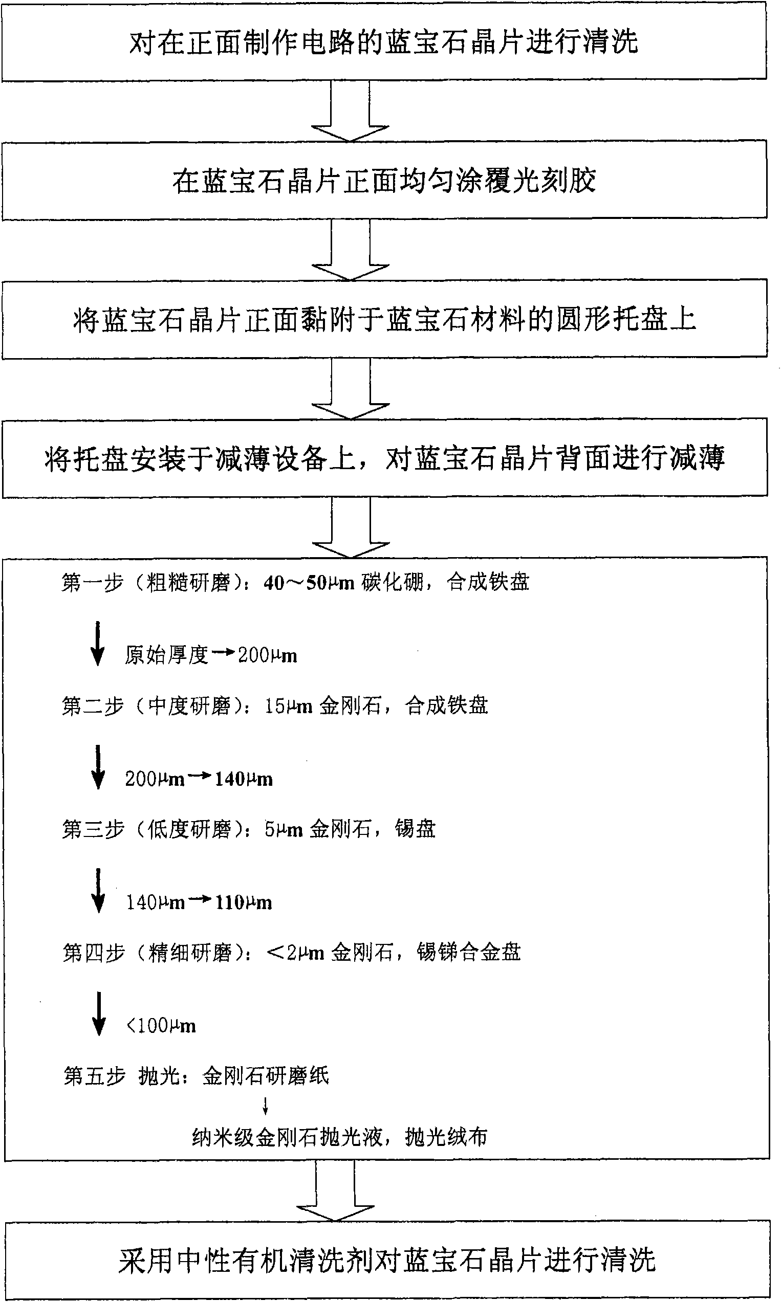
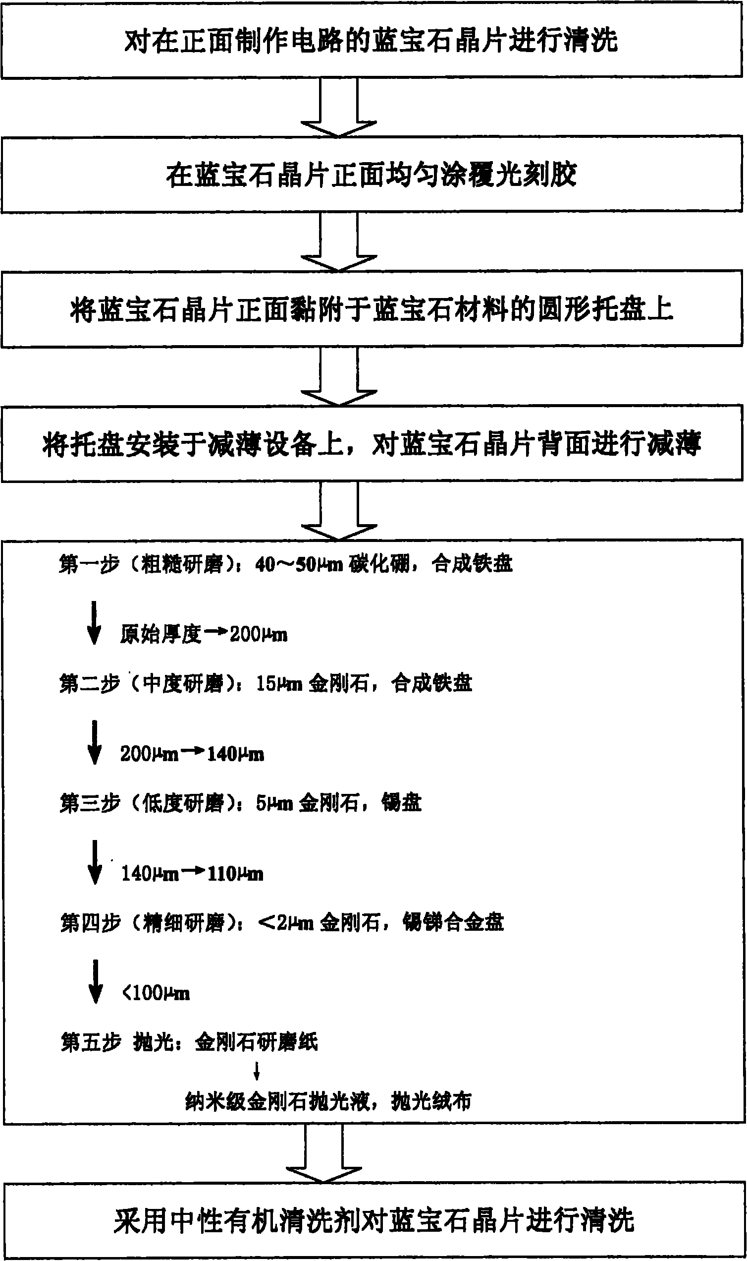
[0031] In order to make the object, technical solution and advantages of the present invention clearer, the present invention will be described in further detail below in conjunction with specific embodiments and with reference to the accompanying drawings.

[0032] Such as figure 1 as shown, figure 1 It is a flow chart of a method for thinning a sapphire wafer provided by the present invention, the method comprising the following steps:

[0033] Step 1: Clean the sapphire wafer on which the circuit is made on the front side;

[0034] Step 2: Coating photoresist evenly on the front of the sapphire wafer, the thickness of the photoresist is 3-5 μm;

[0035] Step 3: Attach the front side of the sapphire wafer to the sapphire round tray;

[0036] Step 4: Install the sapphire round tray on the thinning equipment to thin the back of the sapphire wafer;

[0037] Step 5: Roughly grind the back of the sapphire wafer, including: using boron carbide grinding slurry, combined with a ...


PUM

PropertyMeasurementUnit
thicknessaaaaaaaaaa
Mohs hardnessaaaaaaaaaa

Abstract

The invention discloses a method for thinning a sapphire wafer. The method comprises the following steps: step 1, cleaning a sapphire wafer of which a circuit is made on the front side; step 2, evenly coating a photoresist on the front side of the sapphire wafer; step 3, adhering the front side of the sapphire wafer to a sapphire rounded tray; step 4, installing the sapphire rounded tray on a thinning device to thin the back of the sapphire wafer; step 5, performing a rough grinding on the back of the sapphire wafer; step 6, performing a moderate grinding on the back of the sapphire wafer; step 7, performing a low grinding on the back of the sapphire wafer; step 8, performing fine grinding on the back of the sapphire wafer; step 9, polishing the back of the sapphire wafer; and step 10, washing the sapphire wafer. The method can be used to realize new technique achievements with quick operation, complete wafer structure, no major physical damage, fine and smooth surface and small deformation; and meanwhile, the total thickness of the thinned sapphire wafer is less than 100 mu m.

Description

technical field [0001] The invention relates to the technical field of semiconductors, in particular to a method for thinning a sapphire wafer. Background technique [0002] Gallium nitride (GaN), as the third-generation wide-bandgap semiconductor material, has a large bandgap (3.4eV), a high breakdown voltage (3.3MV / cm), and a high two-dimensional electron gas concentration (>10 13 cm 2 ), high velocity of saturated electrons (2.8×10 7 cm / s) and other characteristics have received extensive attention internationally. The application of GaN in devices is regarded as the most significant event in semiconductors in the 1990s. GaN is a direct bandgap semiconductor material, with a modern width of 3.39eV at room temperature, so it has become a research hotspot of semiconductor materials and optoelectronic devices at home and abroad in recent years. However, because GaN is difficult to prepare bulk materials, it is necessary to epitaxially grow thin films on other substrat...

Claims


Application Information

Patent Timeline
Patent Type & Authority Applications(China)
IPC IPC(8): H01L21/02B28D5/00
Inventor 汪宁陈晓娟罗卫军庞磊刘新宇
Owner INST OF MICROELECTRONICS CHINESE ACAD OF SCI
Why Eureka
Try Eureka