Process method for conformally assembling sip devices on curved surface pcb substrate

A technology of arc-shaped curved surface and process method, which is applied in the manufacturing of semiconductor devices, electric solid-state devices, and semiconductor/solid-state devices, etc., can solve the problem that it is difficult to meet the requirements of SIP packaging and assembly, the heat dissipation capacity of spherical interconnect pins is insufficient, and the top of the device cannot be added. To solve the problems of installing heat dissipation liner, etc., to shorten the development cycle, optimize the shear stress and vibration stress release effect, and achieve good assembly reliability.

Active Publication Date: 2020-05-08
10TH RES INST OF CETC
View PDF6 Cites 0 Cited by
  • Summary
  • Abstract
  • Description
  • Claims
  • Application Information

AI Technical Summary

Problems solved by technology

For circuit design, a three-dimensional chip package will have multiple bare chips stacked. Such a complex package design will bring many problems: such as how to stack multiple chips in one package; Layer substrates, it is difficult to route through traditional tools; there are also issues such as spacing between traces, equal-length design, and differential pair design.
However, there are still many limitations in the use of SIP devices with spherical interconnection pins: 1. SIP devices with spherical interconnection pins are only suitable for the assembly of planar assembly substrates, and for assembly substrate surfaces with curved surfaces that require conformal assembly, due to The spherical interconnection pins are on the same plane, causing the spherical interconnection pins at both ends to contact the curved surface, and the spherical interconnection pins in the middle are suspended, which will lead to poor welding reliability and cannot meet the assembly requirements
like Figure 8 As shown, the SIP device 1 is assembled with the arc-shaped curved surface PCB substrate 3 through the spherical interconnection pin 9, and the pins are suspended, resulting in unreliable assembly.
[0003] 2. For SIP devices with high power and high heat dissipation requirements, due to the insufficient heat dissipation capacity of the spherical interconnection pins and the rigidity of the spherical pins, it is difficult to install a heat dissipation pad on the top of the device to assist heat dissipation, and it is difficult to meet the above-mentioned requirements. Assembly requirements for SIP packages with high power and heat dissipation requirements

Method used


Image

  • Process method for conformally assembling sip devices on curved surface pcb substrate
  • Process method for conformally assembling sip devices on curved surface pcb substrate
  • Process method for conformally assembling sip devices on curved surface pcb substrate

Examples


Embodiment Construction

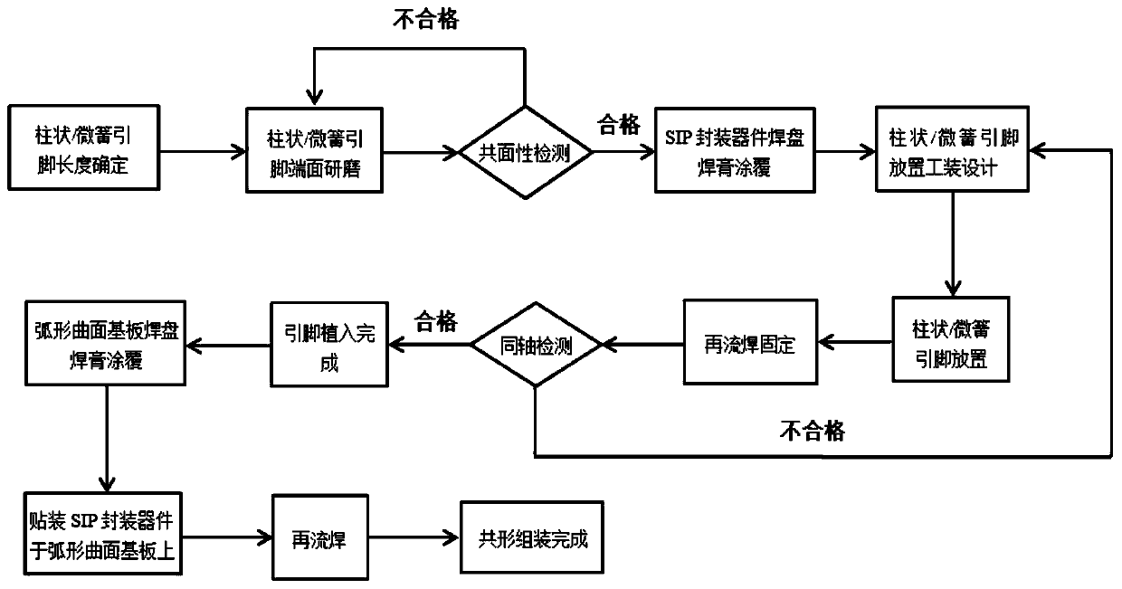
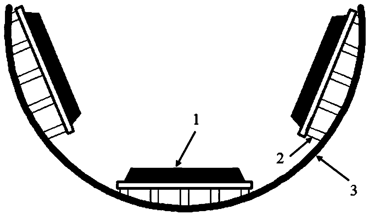
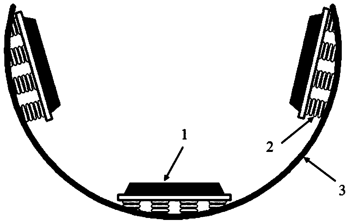
[0018] refer to figure 1 According to the present invention, two new types of interconnection pins (column, microspring form) provided will be implanted into SIP devices and assembled with substrates to realize the technological process of conformal assembly of SIP devices 1 on arc-shaped curved surface PCB substrates 3. The specific implementation method is as follows: : According to the shape and size parameters of the arc-shaped surface of the PCB substrate, determine the length of each columnar or microspring pin that matches it, so as to make columnar or microspring pins 2 with the same or different lengths; for columnar or microspring pins Pin 2 is ground to ensure the coplanar consistency between the end face of the pin and the assembly surface of the substrate, and passes the coplanarity test; solder paste is applied to the pad of the SIP device; it is specially designed for columnar or micro-spring pin 2 The pin placement tooling; place the columnar or micro-spring p...


PUM


Abstract

The invention discloses a process of conformal assembly of an SIP device on a curved surface PCB substrate, and aims at providing a process that reduces the complexity of printed circuit boards, shortens the development cycle and increases the system integration degree. The invention is achieved by the following steps of: packaging a chip into a package in a two-dimensional mode on a same packagesubstrate; using a columnar or micro-spring type pin as an interconnection pin of an SIP device and an external curved surface PCB substrate to produce the columnar or micro-spring type pin that matches the shape of the curved surface PCB substrate; then by a pin placing tool, placing the columnar or micro-spring type pin on a pad of the SIP device in an array form, fixing the pin by welding and performing coaxial detection on the pin; then mounting the SIP device implanted with the columnar or micro-spring type pin therein on the curved surface PCB substrate; and finally completing the conformal assembly of the curved surface PCB substrate and the SIP device by reflow soldering.

Description

technical field [0001] The invention relates to a process method for conformally assembling a SIP device on an arc-shaped curved surface PCB substrate suitable for interconnection and assembly between a System In a Package (SIP) device and an assembly substrate. Background technique [0002] System-in-package (SIP) integrates multiple functional chips, including processors, memory and other functional chips, into one package to achieve a basically complete function. It corresponds to the SOC (System On a Chip) system-on-a-chip. SIP packaging can also integrate passive components, antennas and other system components into a single structure, so that it has more complete system functions. There is no fixed type of SIP package. In many systems, the closed circuit board limits the height and application of SIP. In terms of chip arrangement, the SIP can be a planar 2D package of a Multi-chip Module (MCM), or a 3D package structure can be reused to effectively reduce the package...

Claims


Application Information

Patent Timeline
Patent Type & Authority Patents(China)
IPC IPC(8): H01L21/98
CPCH01L25/50
Inventor 吴军周波
Owner 10TH RES INST OF CETC
Why Eureka
Try Eureka