Semiconductor structure and formation method thereof

A semiconductor and gate structure technology, which is applied in the field of semiconductor structures and their formation, can solve the problems that the electrical properties of semiconductor structures need to be improved, and achieve the effects of avoiding adverse effects, reducing contact resistance, and increasing device drive current

Active Publication Date: 2018-10-23
SEMICON MFG INT (SHANGHAI) CORP +1
View PDF5 Cites 7 Cited by
  • Summary
  • Abstract
  • Description
  • Claims
  • Application Information

AI Technical Summary

Problems solved by technology

[0004] However, the electrical properties of the formed semiconductor structures still need to be improved

Method used


Image

  • Semiconductor structure and formation method thereof
  • Semiconductor structure and formation method thereof
  • Semiconductor structure and formation method thereof

Examples


Embodiment Construction

[0015] It can be seen from the background art that the pre-amorphization implantation process can effectively reduce the height of the Schottky barrier, but the electrical performance of the formed semiconductor structure still needs to be improved. Analyze the reasons for this:

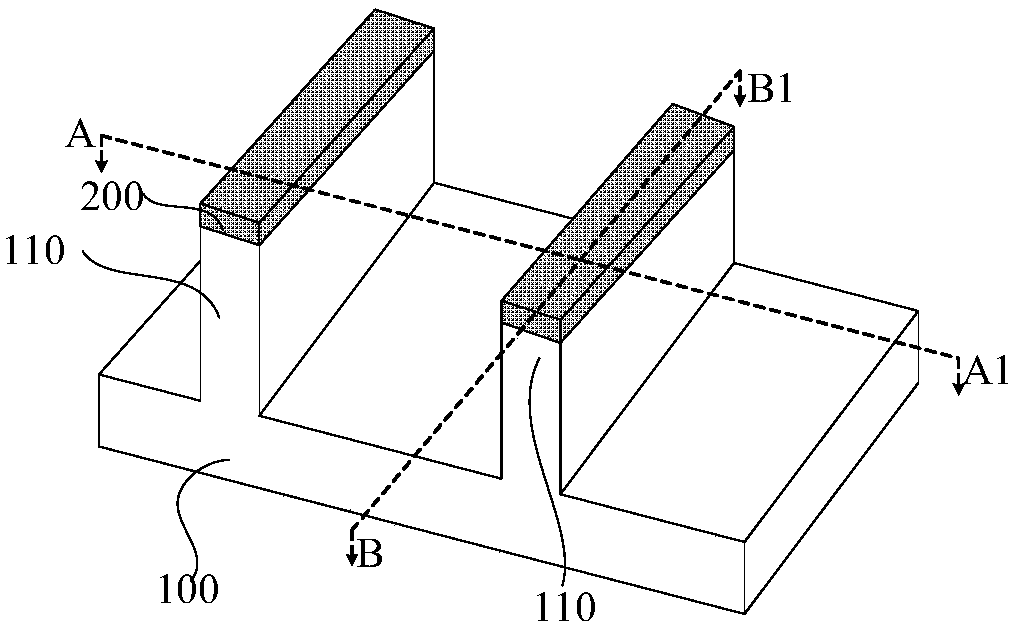
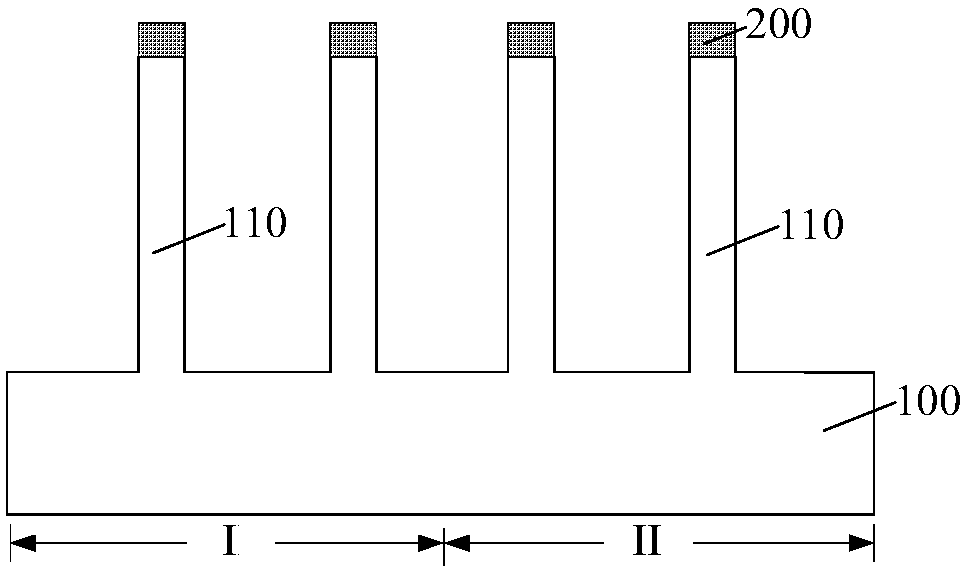
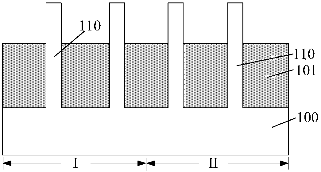
[0016] The contact hole plug of the semiconductor structure includes the first contact hole plug located on the surface of the source and drain doped regions on both sides of the gate structure, which is used to realize the connection between the source region or the drain region of the device and the external circuit; The second contact hole plug on the surface of the pole structure is used to realize the connection between the gate structure and the external circuit. In the formation method of the semiconductor structure, the commonly used method is: after forming the first contact opening exposing the source-drain doped region in the interlayer dielectric layer, firstly pre-discharging the source-...


PUM


Abstract

The invention relates to a semiconductor structure and a formation method thereof. The formation method includes the following steps that: a substrate is provided, gate structures are arranged on thesubstrate, source-drain doping regions located at two sides of each gate structure are formed in the substrate, an interlayer dielectric layer is formed on the substrate which is not covered by the gate structure, and the interlayer dielectric layer covers the tops of the gate structures; first contact openings exposing the source / drain doping regions are formed in the interlayer dielectric layerat two sides of each gate structure; second contact openings which pass through the interlayer dielectric layer above the gate structures are formed; after the second contact openings are formed, pre-amorphization implantation is performed on the source / drain doping regions; after the pre-amorphization implantation process, metal silicide layers are formed at the bottoms of the first contact openings; and after the metal silicide layers are formed, first contact hole plugs are formed in the first contact openings, and second contact hole plugs are formed in the second contact openings. With the formation method of the present invention adopted, amorphous layers formed at the bottoms of the first contact openings can be prevented from being oxidized during the formation of the second contact openings, and therefore, the problem that the metal silicide layers are difficult to form can be avoided.

Description

technical field [0001] The invention relates to the field of semiconductors, in particular to a semiconductor structure and a forming method thereof. Background technique [0002] With the continuous development of integrated circuit manufacturing technology, the critical dimensions of devices are getting smaller and smaller, and many problems have arisen accordingly. For example, the contact resistance between the contact hole plug and the source-drain doped region increases, which leads to a decrease in the response speed of the semiconductor device, a delay in the signal, and a decrease in the driving current, thereby degrading the performance of the semiconductor device. In order to reduce the contact resistance between the contact hole plug and the source-drain doped region, a metal silicide process is introduced. The metal silicide has a lower resistivity and can significantly reduce the contact resistance, thereby increasing the driving current. [0003] With the con...

Claims


Application Information

Patent Timeline
Patent Type & Authority Applications(China)
IPC IPC(8): H01L21/8238H01L27/092
CPCH01L21/823807H01L21/823814H01L21/823821H01L27/0924
Inventor 李勇
Owner SEMICON MFG INT (SHANGHAI) CORP
Why Eureka
Try Eureka