ESD protection circuit, ESD protection structure and forming method thereof

An ESD protection and circuit technology, applied in the direction of circuits, electrical components, electric solid state devices, etc., can solve the problems of poor protection performance of ESD protection circuits

Active Publication Date: 2020-12-25
SEMICON MFG INT (SHANGHAI) CORP +1
View PDF4 Cites 0 Cited by
  • Summary
  • Abstract
  • Description
  • Claims
  • Application Information

AI Technical Summary

Problems solved by technology

[0004] However, the protection performance of the ESD protection circuit formed by the prior art is relatively poor

Method used


Image

  • ESD protection circuit, ESD protection structure and forming method thereof
  • ESD protection circuit, ESD protection structure and forming method thereof
  • ESD protection circuit, ESD protection structure and forming method thereof

Examples


Embodiment Construction

[0038] There are many problems in the semiconductor structure, for example, the protection performance of the ESD protection circuit is poor.

[0039]Combined with a method of forming a semiconductor structure, the reasons for the poor protection performance of the ESD protection circuit are analyzed:

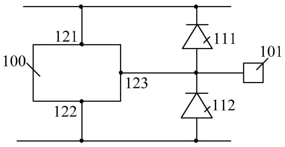
[0040] figure 1 is a circuit diagram of an ESD protection circuit.

[0041] Please refer to figure 1 , the ESD protection circuit includes: a functional device 100, the functional device 100 includes a first end 121, a second end 122 and a connecting portion 123; a pad 101 connected to the connecting portion 123; a first diode 111, The first diode 111 includes a first input part and a first output part, the first input part is connected to the connecting part 123, and the first output part is connected to the first end 121; the second A diode 112 , the second diode 112 includes a second input part and a second output part, the second input part is grounded, and the second ou...


PUM


Abstract

The invention provides an ESD protection circuit, an ESD protection structure and a formation method thereof. The circuit comprises a function device, a first semiconductor transistor, a second semiconductor transistor and a third semiconductor transistor, wherein the function device includes a device output end, a device input end and a connection end; the first semiconductor transistor includesa first input end and a first output end; the first input end is connected to the device output end, and the first output end is connected to the device input end; and when the potential of the firstoutput end is higher than the potential of the first input end, and the potential difference between the first output end and the first input end is greater than the threshold conduction voltage of the first semiconductor transistor, the first semiconductor transistor is conducted. The ESD protection circuit comprises the first semiconductor transistor. When an electric charge quantity on a firstbonding pad is large, electric charges on the first bonding pad can be released through the first semiconductor transistor so that the pathway of charge releasing can be increased and the performanceof the ESD protection circuit is improved.

Description

technical field [0001] The invention relates to the technical field of semiconductor manufacturing, in particular to an ESD protection circuit, an ESD protection structure and a forming method thereof. Background technique [0002] Static electricity is an objectively existing natural phenomenon, which can be produced in many ways, such as contact, friction, induction between electrical appliances, etc. Static electricity has the characteristics of long-term accumulation, high voltage, low power, low current and short action time. [0003] For electronic products, electrostatic discharge (Electrostatic discharge, ESD) is a major factor affecting the reliability of integrated circuits. ESD is a rapid neutralization process of electric charge. Due to the high electrostatic voltage, it will bring destructive consequences to the integrated circuit, resulting in the failure of the integrated circuit. Therefore, in order to protect the integrated circuit from being damaged by E...

Claims


Application Information

Patent Timeline
Patent Type & Authority Patents(China)
IPC IPC(8): H01L27/02
CPCH01L27/0251
Inventor 雷玮李宏伟罗婵季林燕
Owner SEMICON MFG INT (SHANGHAI) CORP
Why Eureka
Try Eureka