Bonded body, substrate for power module, power module, method for manufacturing the bonded body, and method for manufacturing substrate for power module
A manufacturing method and technology for power modules, which are applied in semiconductor/solid-state device manufacturing, manufacturing tools, welding/welding/cutting items, etc., can solve the problems of large thermal stress on ceramic substrates, high heating temperature, and hard intermetallic compounds, etc. To achieve the effect of suppressing partial discharge
- Summary
- Abstract
- Description
- Claims
- Application Information
AI Technical Summary
Problems solved by technology
Method used
Image

Examples
no. 1 approach
[0056] Hereinafter, embodiments of the present invention will be described with reference to the drawings. First, a first embodiment of the present invention will be described.
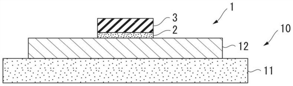
[0057] The bonded body according to the present embodiment is a power module substrate 10 formed by bonding ceramic substrate 11 which is a ceramic component and Cu plate 22 (circuit layer 12 ) which is a Cu component. figure 1 A power module 1 including a power module substrate 10 according to the present embodiment is shown in FIG.
[0058] The power module 1 includes: a power module substrate 10 provided with a circuit layer 12; and a semiconductor element 3 bonded to one side of the circuit layer 12 via a solder layer 2 (in figure 1 Middle is the upper surface).
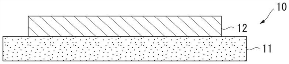
[0059] Such as figure 2 As shown, the power module substrate 10 includes a ceramic substrate 11 and one side of the ceramic substrate 11 (in figure 2 The middle is the circuit layer 12 on the upper surface).
[0060] The ceramic s...
no. 2 approach
[0098] Next, a second embodiment of the present invention will be described. In addition, the same code|symbol is used for the same structure as 1st Embodiment, and detailed description is abbreviate|omitted.
[0099] Figure 6 A power module 101 including a power module substrate 110 according to the second embodiment is shown.
[0100] The power module 101 includes: a power module substrate 110 on which a circuit layer 112 and a metal layer 113 are disposed; and a semiconductor element 3 bonded to one side of the circuit layer 112 via a solder layer 2 ( Figure 6 middle is the upper surface); and the heat sink 130 is configured on the other side of the metal layer 113 (in Figure 6 Middle is the lower side).
[0101] Such as Figure 7 As shown, the power module substrate 110 includes: a ceramic substrate 11; a circuit layer 112 disposed on one side of the ceramic substrate 11 (in Figure 7 The middle is the upper surface); and the metal layer 113 is arranged on the othe...
no. 3 approach
[0126] Next, a third embodiment of the present invention will be described. In addition, the same code|symbol is used for the same structure as 1st Embodiment, and detailed description is abbreviate|omitted.
[0127] Figure 11 A power module 201 including a power module substrate 210 according to the third embodiment is shown.
[0128] The power module 201 includes: a power module substrate 210 on which a circuit layer 212 and a metal layer 213 are disposed; and a semiconductor element 3 bonded to one side of the circuit layer 212 via a solder layer 2 ( Figure 11 The middle is the upper surface); and the heat sink 230 is bonded to the other side of the power module substrate 210 (in Figure 11 Middle is the lower side).
[0129] Such as Figure 12 As shown, the power module substrate 210 includes: a ceramic substrate 11; a circuit layer 212 disposed on one side of the ceramic substrate 11 (in Figure 12 The middle is the upper surface); and the metal layer 213 is arrang...
PUM
| Property | Measurement | Unit |
|---|---|---|
| thickness | aaaaa | aaaaa |
| thickness | aaaaa | aaaaa |
| thickness | aaaaa | aaaaa |
Abstract
Description
Claims
Application Information
 - R&D
- Intellectual Property
- Life Sciences
- Materials
- Tech Scout
- Unparalleled Data Quality
- Higher Quality Content
- 60% Fewer Hallucinations
Browse by: Latest US Patents, China's latest patents, Technical Efficacy Thesaurus, Application Domain, Technology Topic, Popular Technical Reports.
© 2025 PatSnap. All rights reserved.Legal|Privacy policy|Modern Slavery Act Transparency Statement|Sitemap|About US| Contact US: help@patsnap.com