Micro-displayer pixel circuit

A micro-display and pixel circuit technology, applied in the field of pixel circuits, can solve problems such as complex peripheral circuits, slow charging speed, and difficult control of the working range of sub-threshold regions

Pending Publication Date: 2018-11-09
LUMICORE MICROELECTRONICS SHANGHAI CO LTD
View PDF8 Cites 3 Cited by
  • Summary
  • Abstract
  • Description
  • Claims
  • Application Information

AI Technical Summary

Problems solved by technology

Existing micro-displays based on single crystal silicon use sub-threshold voltage scaling technology to generate tiny currents to drive tiny pixels of micro-displays. Level current, but t

Method used


Image

  • Micro-displayer pixel circuit
  • Micro-displayer pixel circuit
  • Micro-displayer pixel circuit

Examples


no. 1 example

[0057] This embodiment illustrates different schemes of the pixel circuit of the microdisplay according to the present invention.

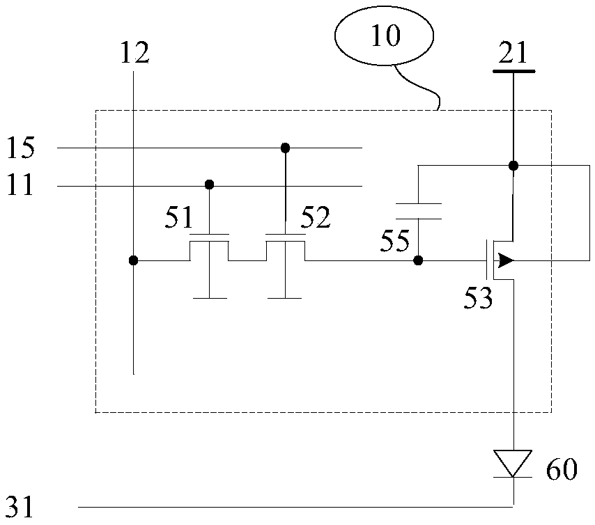
[0058]In the first solution, as shown in Figure 1(a), the pixel circuit 10 includes a series transistor 51, a series transistor 52, a first drive transistor 53, and a capacitor 55; the gate of the series transistor 51 is connected to the first gate Line 11, the gate of the series transistor 52 is connected to the second gate line 15; the source (or drain) of the series transistor 51 is connected to the data line 12, and the drain (or source) of the series transistor 51 is connected to the series transistor 52 source (or drain), the drain (or source) of the series transistor 52 is connected to the gate of the first driving transistor 53; the first driving transistor 53 is a P-type transistor, and the source is connected to the pixel power supply 21. The drain is connected to one end of the light emitting device 60 (anode in the figure), and the sub...

no. 2 example

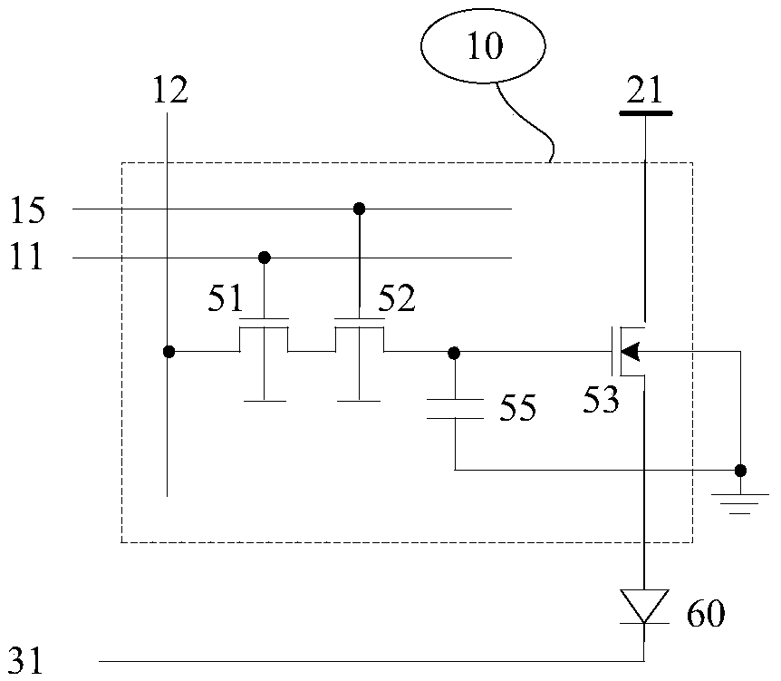
[0070] In the first solution, as shown in Figure 3(a), the pixel circuit 10 includes a series transistor 51, a series transistor 52, a series transistor 56, a first drive transistor 53, a first control transistor 54, and a capacitor 55; the series transistor The gate of the series transistor 51 is connected to the first gate line 11, the gate of the series transistor 52 is connected to the second gate line 15, and the gate of the series transistor 56 is connected to the third gate line 16; the source of the series transistor 51 ( or drain) is connected to the data line 12, the drain (or source) of the series transistor 51 is connected to the source (or drain) of the series transistor 52, and the drain (or source) of the series transistor 52 is connected to the series transistor 56 source (or drain), the drain (or source) of the series transistor 56 is connected to the gate of the first driving transistor 53; the first driving transistor 53 is a P-type transistor, and its source...

no. 3 example

[0086] This embodiment illustrates different schemes of the pixel circuit of the microdisplay according to the present invention.

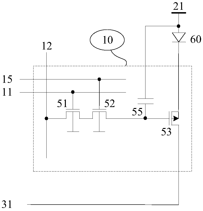
[0087] In the first solution, as shown in Figure 4(a), the pixel circuit 10 includes a first transistor 57, a second transistor 59, a first drive transistor 53, and a capacitor 55; the first transistor 57 is a P-type transistor, and its The gate is connected to the gate line 17, and the substrate is connected to the pixel power supply 21; the second transistor 59 is an N-type transistor, and its gate is connected to the gate line 19, and the substrate is connected to the ground; the source of the first transistor 57 pole (or drain) is connected to the drain (or source) of the second transistor 59 and the data line 12, and the drain (or source) of the first transistor 57 is connected to the source (or drain) of the second transistor 59 ) and the gate of the first drive transistor 53; the first drive transistor 53 is a P-type transistor, the source ...


PUM


Abstract

The invention discloses a micro-displayer pixel circuit. The pixel circuit comprises N series connected transistors, a first driving transistor and a capacitor or comprises N series connected transistors, a first driving transistor and M control transistors connected in series with the first driving transistor and a capacitor or comprises a first transistor, a second transistor, a first driving transistor and a capacitor or comprises a first transistor, a second transistor, a first driving transistor and M control transistors connected in series with the first driving transistor and a capacitor. The topology structure and the working mode of the pixel circuit are disclosed, and the pixel circuit has the advantages of high charging speed, simple peripheral circuit, low electric leakage andhigh accuracy and stability and enhancing maximum brightness and contrast in comparison with those of the present scheme.

Description

technical field [0001] The invention relates to the technical field of plane displays, in particular to a pixel circuit for a microdisplay with a single crystal silicon chip as a substrate. Background technique [0002] Contemporary flat-panel displays generally use polysilicon or amorphous silicon as a substrate, and driving circuits are integrated on the polysilicon or amorphous silicon substrate to generate the current or voltage required by the light emitting device. In an actively driven display panel, each pixel has an independent pixel circuit. When the pixel panel is further reduced, monocrystalline silicon is used as the substrate to form a micro-display with a diagonal size of less than 1 inch, and a pixel pitch of more than 2000PPI (pixels per inch). Since the characteristic size of transistors in monocrystalline silicon is much smaller than that of transistors in polycrystalline silicon or amorphous silicon substrates, the driving circuit of monocrystalline sili...

Claims


Application Information

Patent Timeline
IPC IPC(8): G09G3/20
CPCG09G3/20
Inventor 季渊王成刘万林穆廷洲沈伟星黄舒平
Owner LUMICORE MICROELECTRONICS SHANGHAI CO LTD
Why Eureka
Try Eureka