Simulation method and system and wiring structure of DDR circuit
A simulation method and simulation system technology, applied in electrical digital data processing, special data processing applications, instruments, etc., can solve the problems of reducing the signal quality of DDR circuits, discontinuous target impedance of signal links, affecting the signal integrity of DDR circuits, etc. , to achieve the effect of ensuring signal integrity, impedance continuity, and improving signal quality
- Summary
- Abstract
- Description
- Claims
- Application Information
AI Technical Summary
Problems solved by technology
Method used
Image
Examples
Embodiment 1
[0029] This embodiment provides a method for emulating a DDR circuit, which can be applied to any terminal device capable of running a DDR circuit emulation application or program, such as a PC (Personal Computer, personal computer) client, server, dedicated data processing device, etc. , and may also be a mobile terminal such as a mobile phone, a tablet computer, a personal digital assistant, or a notebook computer.
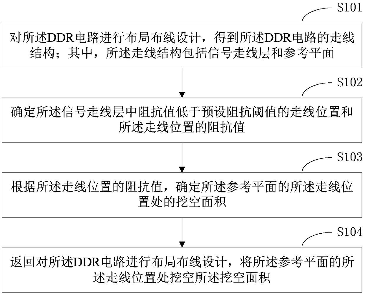
[0030] Such as figure 1 As shown, the simulation method of the DDR circuit provided in this embodiment includes:
[0031] Step S101 , performing layout and wiring design on the DDR circuit to obtain a wiring structure of the DDR circuit; wherein, the wiring structure includes a signal wiring layer and a reference plane.
[0032] In a specific application, before the layout and wiring design of the DDR circuit, it is necessary to determine the topology type and characteristic impedance value of the routing structure of the DDR circuit. The topology type includes...
Embodiment 2
[0063] This embodiment provides a DDR circuit emulation system for executing the method steps in Embodiment 1. The system may be a software program system in any terminal device capable of running a DDR circuit emulation application or program.
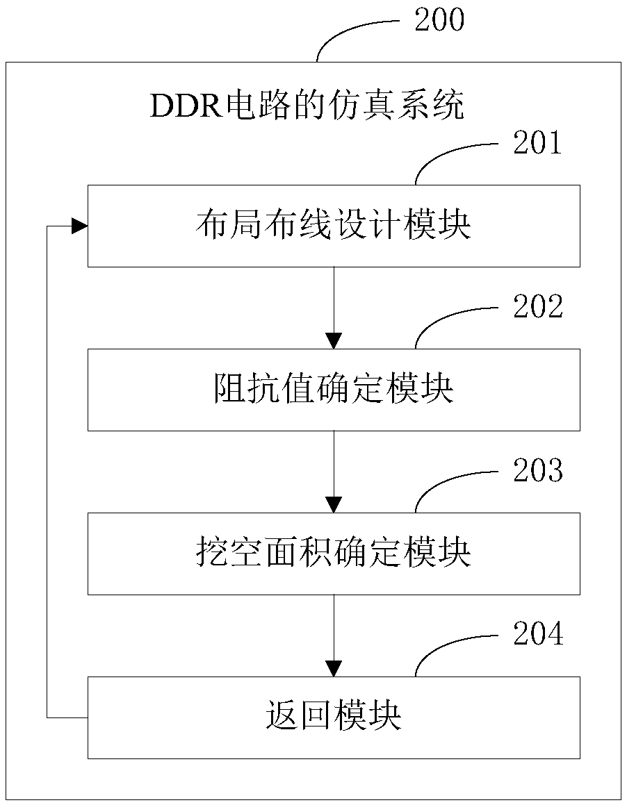
[0064] Such as figure 2 As shown, the simulation system 200 of the DDR circuit provided in this embodiment includes:
[0065] The layout and wiring design module 201 is configured to perform layout and layout design on the DDR circuit to obtain the wiring structure of the DDR circuit; wherein, the wiring structure includes a signal wiring layer and a reference plane;
[0066] An impedance value determination module 202, configured to determine a trace position in the signal trace layer whose impedance value is lower than a preset impedance threshold and an impedance value of the trace position;
[0067] A hollowed out area determination module 203, configured to determine the hollowed out area at the traced position of the reference...
Embodiment 3
[0085] Such as image 3 As shown, this embodiment provides a routing structure 300 of a DDR circuit implemented based on the simulation method of Embodiment 1 or the simulation system of Embodiment 2, which includes a signal routing layer 301 and a reference plane 302 .
[0086] In a specific application, the routing structure 300 may include two or more layers according to actual needs, and the specific number of layers may be designed according to actual layout and wiring needs. image 3 Only the parts related to this embodiment are shown in , and are not used to limit the actual implementation form of the wiring structure 300 .
[0087] Such as image 3 As shown, in this embodiment, a through hole 3021 with an area equal to the hollowed-out area is opened at the routing position 3011 of the reference plane 302;
[0088] The signal routing layer 301 has a via hole, and the routing position 3011 is the location of the via hole, that is, the routing position 3011 is the via ...
PUM
 Abstract
Description
Claims
Application Information


