Manufacturing method of array substrate, array substrate and display panel

A technology for array substrates and manufacturing methods, which is applied in the display field and can solve problems such as difficulty in controlling the uniformity of the gate insulating layer, uneven electrical properties, and difficulty in taking into account the uniformity of the gate insulating layer, etc.

Inactive Publication Date: 2018-11-13
WUHAN CHINA STAR OPTOELECTRONICS TECH CO LTD
View PDF6 Cites 1 Cited by
  • Summary
  • Abstract
  • Description
  • Claims
  • Application Information

AI Technical Summary

Problems solved by technology

The inventors of the present application further found that due to sequential etching of metals and non-metals, it is difficult to take into account the uniformity of the gate line width and the etched gate insulating layer, and thus the uniformity of the remaining gate insulating layer is extremely difficult to control. Easy to cause electrical unevenness

Method used


Image

  • Manufacturing method of array substrate, array substrate and display panel
  • Manufacturing method of array substrate, array substrate and display panel
  • Manufacturing method of array substrate, array substrate and display panel

Examples


Embodiment Construction

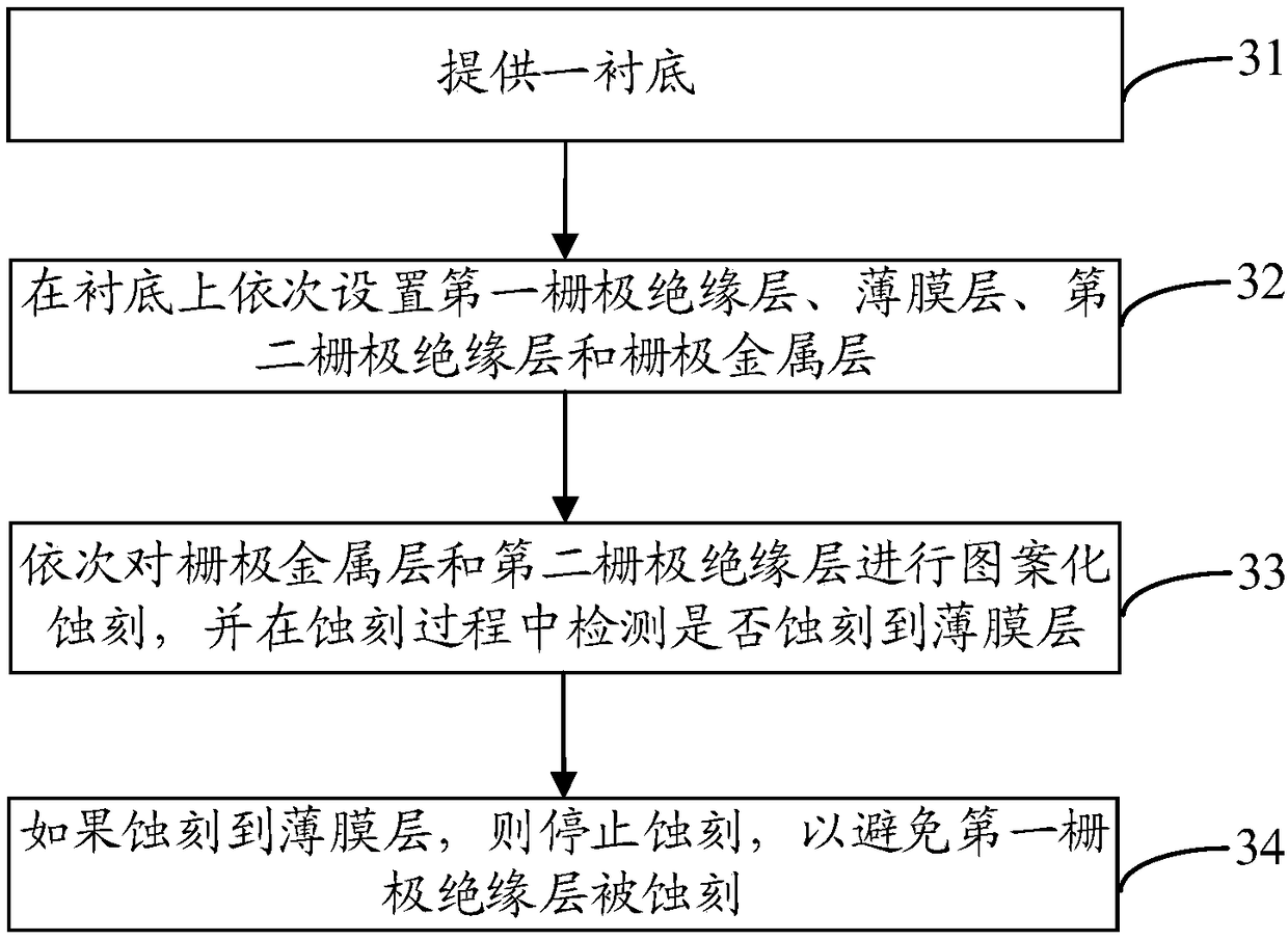
[0021] The following will clearly and completely describe the technical solutions in the embodiments of the present application with reference to the drawings in the embodiments of the present application. Obviously, the described embodiments are only some of the embodiments of the present application, not all of them. Based on the embodiments in this application, all other embodiments obtained by persons of ordinary skill in the art without making creative efforts belong to the scope of protection of this application.

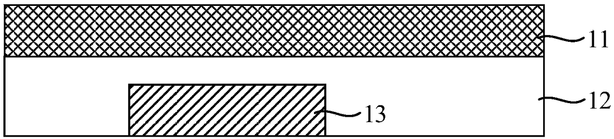
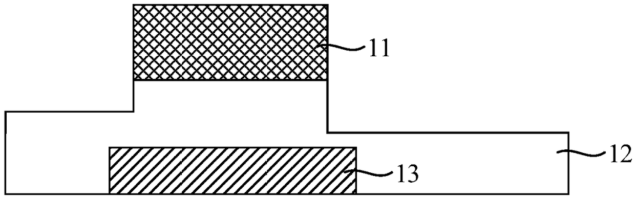
[0022] The film layer structure before gate etching is as follows: figure 1 As shown, since the gate metal layer 11 needs to be etched, and then the gate insulating layer 12 is etched, which involves metal and non-metal etching, it is difficult to ensure the uniformity of the etched gate insulating layer 12, which is formed as follows figure 2 In the structure shown, the upper surface of the gate insulating layer 12 not covered by the gate metal layer 11 is n...


PUM


Abstract

The invention discloses a manufacturing method of an array substrate, the array substrate and a display panel. The method comprises steps as follows: providing a substrate; sequentially arranging a first gate insulation layer, a film layer, a second gate insulation layer and a gate metal layer on the substrate; sequentially performing pattern etching on the gate metal layer and the second gate insulation layer, and detecting whether the film layer is etched in the etching process; if the film layer is etched, stopping etching to prevent the first gate insulation layer from being etched, wherein the material of the film layer is different from that of the second gate insulation layer. With the adoption of the scheme, the ion implantation uniformity can be improved, and the electric stability can be enhanced.

Description

technical field [0001] The present application relates to the field of display technology, in particular to a method for manufacturing an array substrate, an array substrate and a display panel. Background technique [0002] LTPS (Low Temperature Poly-silicon, low-temperature polysilicon) technology has gradually matured and is widely used in high-resolution products such as mobile phones. The current LTPS process is complicated, and the equipment is very precise and expensive. Therefore, in order to increase production capacity and reduce costs, it can only be saved through technological improvement mask to achieve. Re-etch technology can increase the production capacity of photoresist strippers, so many manufacturers are actively researching this technology in order to maximize production capacity. [0003] The inventors of the present application found in the long-term research and development that there are also some defects in the re-etching technology, mainly because ...

Claims


Application Information

Patent Timeline
IPC IPC(8): H01L27/12H01L21/77G02F1/13G02F1/1362
CPCG02F1/1303G02F1/1362H01L27/1214H01L27/1259
Inventor 黄奔
Owner WUHAN CHINA STAR OPTOELECTRONICS TECH CO LTD
Why Eureka
Try Eureka