Semiconductor device

A semiconductor and conductive technology, which is applied in the manufacture/processing of electromagnetic devices, electrical solid devices, electrical components, etc., can solve the problems that the depletion layer expansion mode is difficult to be uniform, and the offset voltage residue cannot be eliminated, so as to reduce the characteristic deviation , the effect of uniform expansion mode

Inactive Publication Date: 2018-11-13
SII SEMICONDUCTOR CORP
View PDF2 Cites 0 Cited by
  • Summary
  • Abstract
  • Description
  • Claims
  • Application Information

AI Technical Summary

Problems solved by technology

However, in the Hall element disclosed in Patent Document 1, as described above, it is difficult to spread the depletion layer uniformly.
Therefore, when switching the direction of flowing current (current application direction) in the case of performing offset cancellation by the spinning current method in the Hall element of Patent Document 1, the expansion mode of the depletion layer generated in each current application direction different, therefore, it is impossible to eliminate the offset voltage while residual

Method used


Image

  • Semiconductor device
  • Semiconductor device
  • Semiconductor device

Examples


no. 4 approach

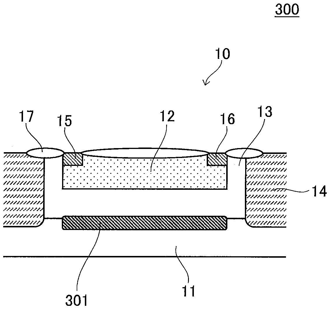
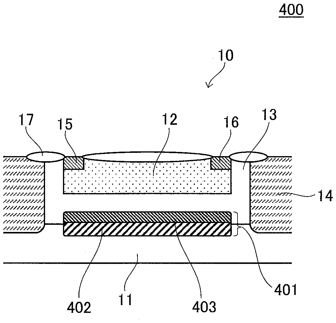
[0038] Therefore, as the second to fourth embodiments of the present invention, structures for further reducing junction leakage at high temperatures while maintaining the above-mentioned effects obtained in the semiconductor device 100 of the first embodiment will be described below.

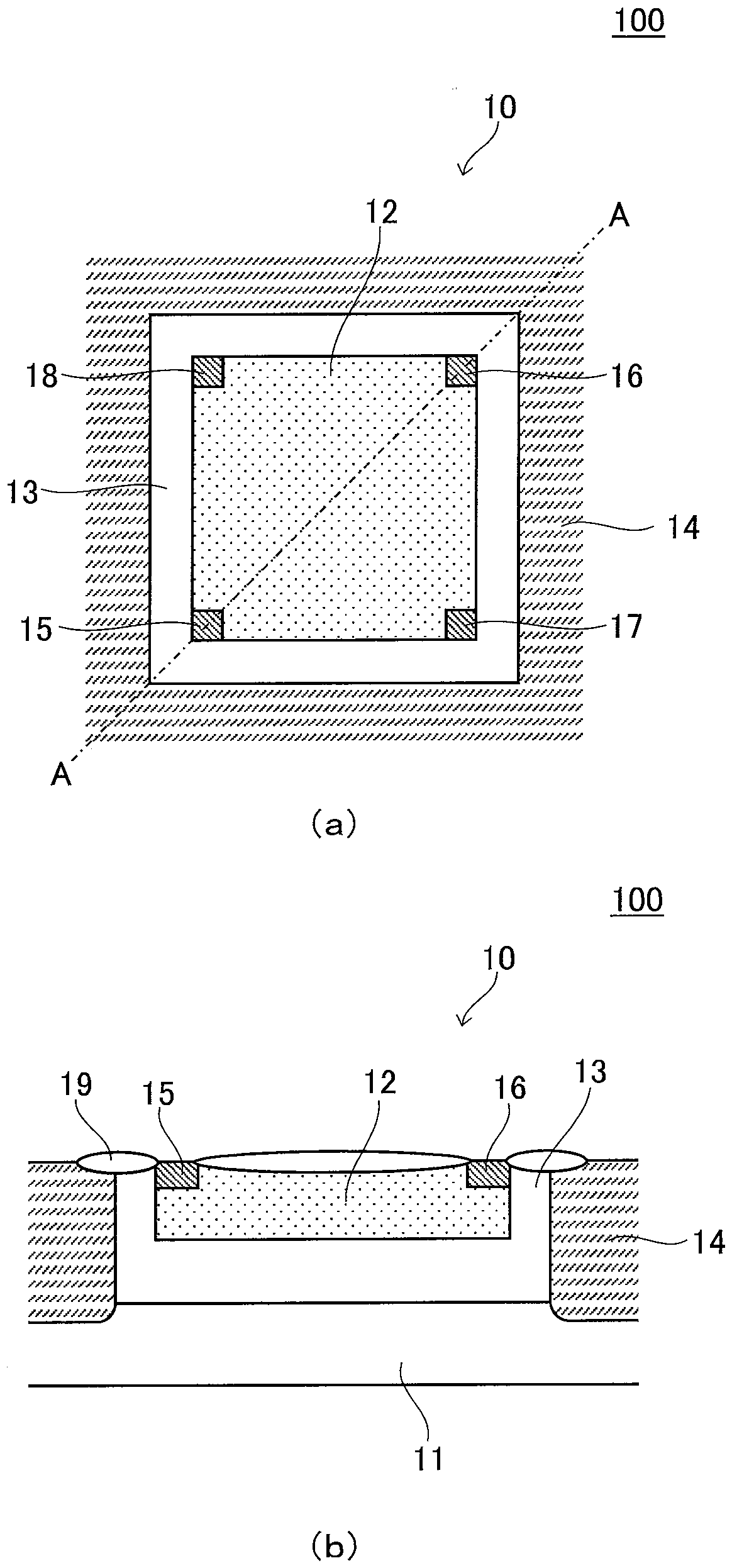
[0039] Figure 2~4 It is a sectional view for respectively explaining the semiconductor devices 200-400 of 2nd - 4th Embodiment of this invention. About each plan view of semiconductor device 200-400, and figure 1 The plan view of (a) corresponds, therefore, the illustration is omitted.

[0040] again, yes and figure 1 The same constituent elements of the illustrated semiconductor device 100 are denoted by the same reference numerals, and overlapping descriptions are appropriately omitted.

[0041] The semiconductor device 200 of the second embodiment is as figure 2 As shown, in the semiconductor device 100 of the first embodiment, a P-type buried layer 201 is further provided between the ...


PUM


Abstract

The invention relates to a semiconductor device. Provided is a semiconductor device including a Hall element, in which a depletion layer is prevented from spreading to a magnetism sensing portion morereliably, and thus variations in characteristic are reduced. The semiconductor device includes: a semiconductor substrate of a first conductivity type; and a Hall element formed on the semiconductorsubstrate, the Hall element having: a magnetism sensing portion of a second conductivity type formed on the semiconductor substrate so as to be separated from the semiconductor substrate; and a semiconductor layer of the second conductivity type formed so as to surround side surfaces and a bottom surface of the magnetism sensing portion on the semiconductor substrate and has a lower concentrationthan a concentration of the magnetism sensing portion and a uniform concentration distribution.

Description

technical field [0001] The present invention relates to a semiconductor device, and more particularly, to a semiconductor device having a Hall element that senses a magnetic field in a direction perpendicular to a semiconductor substrate. Background technique [0002] Since the Hall element can detect a magnetic field using the Hall effect, and can sense a position or an angle in a non-contact manner by being used as a magnetic sensor, it is used in various applications. Transverse Hall elements capable of detecting a magnetic field in a vertical direction are generally known widely. [0003] The lateral Hall element includes, for example, a magnetic sensing part provided on a semiconductor substrate, a pair of input electrodes and a pair of output electrodes provided on the surface of the magnetic sensing part. [0004] Then, when a magnetic field is applied to the semiconductor substrate in a vertical direction and a current flows between the pair of input electrodes, a L...

Claims


Application Information

Patent Timeline
Patent Type & Authority Applications(China)
IPC IPC(8): H01L43/06
CPCH10N52/101H10N52/80H10N52/01
Inventor 小川洋平飞冈孝明
Owner SII SEMICONDUCTOR CORP
Why Eureka
Try Eureka