SERS (Surface Enhanced Raman Scattering) unit, and preparation method and application thereof
An etching method, nanoparticle technology, applied in surface reactive electrolytic coating, nanotechnology for sensing, nanotechnology for materials and surface science, etc. application and other issues, to achieve the effects of low preparation cost, high uniformity and convenient operation
- Summary
- Abstract
- Description
- Claims
- Application Information
AI Technical Summary
Problems solved by technology
Method used
Image
Examples
preparation example Construction
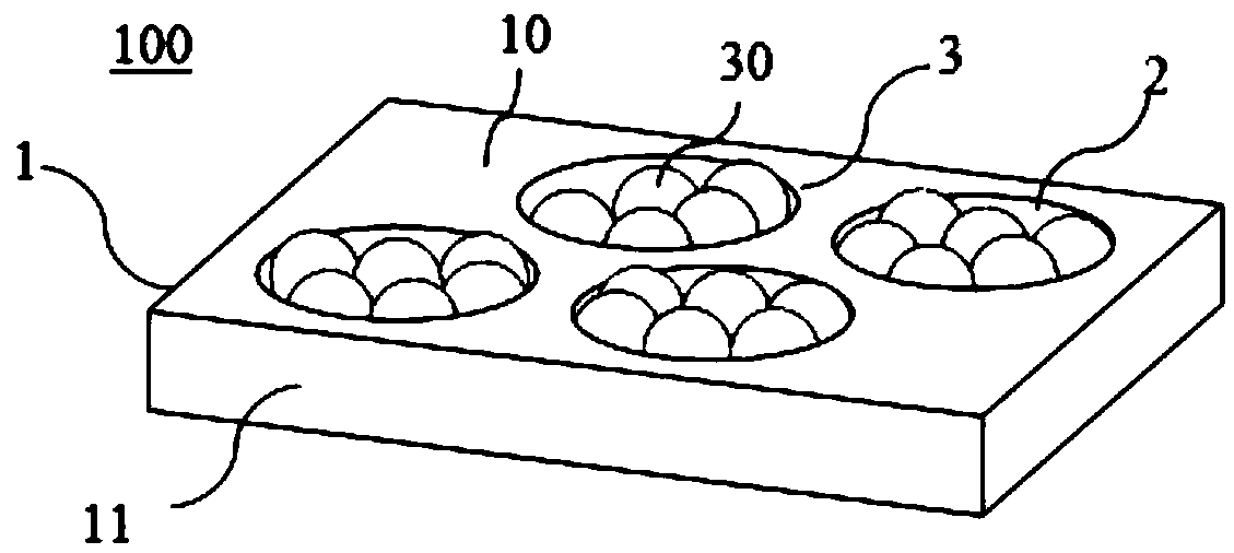
[0053] In some embodiments, the preparation method of the SERS unit of the present invention includes: firstly, a porous metal oxide layer is made on the surface of the metal substrate by electrochemical anodic oxidation, so that the metal substrate becomes the first layer composed of metal and composed of metal oxide to form a SERS unit substrate with a plurality of nano-depressions on the surface. Secondly, the SERS unit substrate is immersed in a dispersion liquid dispersed with specific concentrations of SERS active nanoparticles, and the SERS active nanoparticles are self-assembled into multiple nano-depressions to form nanoparticle aggregates limited by the nano-depressions. The size of the nanoparticle aggregate and the number of nanoparticles contained in the nanoparticle aggregate can be controlled by the concentration of the nanoparticle dispersion, self-assembly time and other conditions. Preferably, the preparation method may further include: controlling the time f...
Embodiment 1
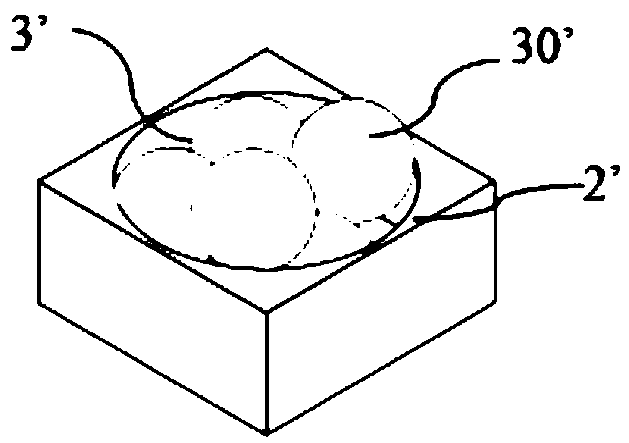
[0065] This embodiment provides a SERS chip, which is composed of one SERS unit. The size of the SERS unit is 4mm*4mm, the SERS unit includes a substrate with a plurality of nano-depressions discretely distributed on the surface, and nano-particle aggregates dispersed in the nano-depressions, each nano-particle aggregate is composed of a plurality of nano-particles Aggregations are formed, and each nanoparticle aggregate is confined by a corresponding nano-depression.
[0066] The SERS unit was prepared by the following steps:
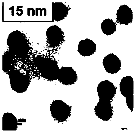
[0067] (1) Provide the substrate: take the alumina template prepared by the anodic oxidation method (the thickness is 0.3mm, and its SEM image is as follows Figure 5 As shown, a plurality of nano-depressions are microscopically disordered and macroscopically uniformly distributed on the entire surface of the substrate, and the number of nano-depressions per square centimeter on the substrate is about 10 8 ~10 9 One, the diameter of the nano-depress...
Embodiment 2
[0072] This embodiment provides a SERS chip, which is basically the same as in Embodiment 1, except that the dipping time is controlled to be 4h during preparation. The SEM image of the SERS chip obtained in this example is as follows Figure 9 As shown, it can be seen that nanoparticle aggregates are formed in each nano-depression, most of the nanoparticle aggregates contain a plurality of spherical nanoparticles aggregated together, and the number of nanoparticles contained in each nanoparticle aggregate is 6 to 10 pieces, the average number is about 8 pieces. Nanoparticles in each nanodepression are basically arranged in a single layer.
PUM
| Property | Measurement | Unit |
|---|---|---|
| depth | aaaaa | aaaaa |
| diameter | aaaaa | aaaaa |
| particle diameter | aaaaa | aaaaa |
Abstract
Description
Claims
Application Information
 - R&D
- Intellectual Property
- Life Sciences
- Materials
- Tech Scout
- Unparalleled Data Quality
- Higher Quality Content
- 60% Fewer Hallucinations
Browse by: Latest US Patents, China's latest patents, Technical Efficacy Thesaurus, Application Domain, Technology Topic, Popular Technical Reports.
© 2025 PatSnap. All rights reserved.Legal|Privacy policy|Modern Slavery Act Transparency Statement|Sitemap|About US| Contact US: help@patsnap.com


