Formation method of fin type field effect transistor structure

A fin field effect and transistor technology, which is applied in semiconductor devices, semiconductor/solid state device manufacturing, electrical components, etc., can solve the problem of poor control of height and width, poor fin shape uniformity, and threshold voltage of fin field effect transistors. Offset and other issues, to achieve short cycle, reduce the difficulty of etching process, reduce the effect of process cost

Active Publication Date: 2018-11-20
SHANGHAI INTEGRATED CIRCUIT RES & DEV CENT
View PDF8 Cites 0 Cited by
  • Summary
  • Abstract
  • Description
  • Claims
  • Application Information

AI Technical Summary

Problems solved by technology

However, the height and width of the fins formed by this method are not well controlled; and the shape uniformity of the edges and sidewalls of the formed fins is poor
This will shift the threshold voltage of the FinFET and affect the stability of the FinFET

Method used


Image

  • Formation method of fin type field effect transistor structure
  • Formation method of fin type field effect transistor structure
  • Formation method of fin type field effect transistor structure

Examples


Embodiment Construction

[0032] The specific embodiment of the present invention will be further described in detail below in conjunction with the accompanying drawings.

[0033] It should be noted that, in the following specific embodiments, when describing the embodiments of the present invention in detail, in order to clearly show the structure of the present invention for the convenience of description, the structures in the drawings are not drawn according to the general scale, and are drawn Partial magnification, deformation and simplification are included, therefore, it should be avoided to be interpreted as a limitation of the present invention.

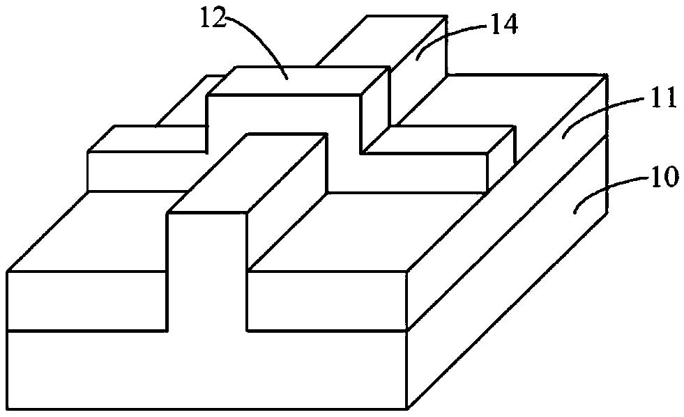
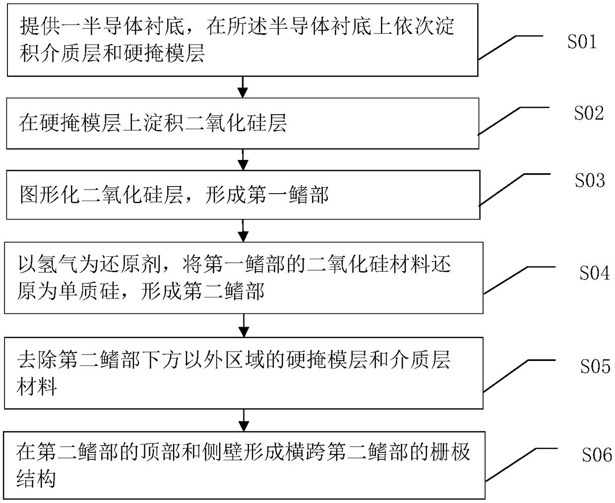
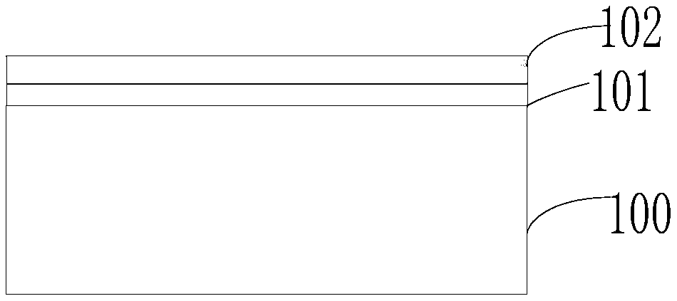
[0034] In the following specific embodiments of the present invention, please refer to figure 2 , figure 2 It is a schematic flow chart of a method for forming a fin field effect transistor structure according to a preferred embodiment of the present invention; meanwhile, please refer to Figure 3 ~ Figure 9 , Figure 3 ~ Figure 9 is based on ...


PUM


Abstract

The invention discloses a formation method of a fin type field effect transistor structure, comprising the following steps: S01, providing one semiconductor substrate, and sequentially depositing a dielectric layer and a hard mask layer on the semiconductor substrate; S02, depositing a silicon dioxide layer on the hard mask layer; S03, performing graphical processing on the silicon dioxide layer,and forming a first fin part; S04, taking hydrogen as a reducing agent, and reducing a silicon dioxide material of the first fin part into monatomic silicon, so as to form a second fin part; S05, removing the hard mask layer and a dielectric layer material in regions except a region below the second fin part; and S06, forming a grid structure crossing the second fin part at the top and on the sidewall of the second fin part. The formation method disclosed by the invention avoids direct etching on a silicon material, reduces difficulty of an etching process, can accurately control width and height of each fin part, can be compatible with the conventional silicon-based ultra large scale integrated circuit manufacturing technology and has the characteristics of simplicity, convenience and short cycle, and process cost is reduced.

Description

technical field [0001] The present invention relates to the technical field of integrated circuit manufacturing, and more particularly, to a method for forming a Fin Field Effect Transistor structure. Background technique [0002] With the continuous development of semiconductor technology, traditional planar devices have been difficult to meet people's demand for high-performance devices. [0003] A Fin Field-Effect Transistor (Fin Field-Effect Transistor, FinFET) is a three-dimensional device, including fins vertically formed on a substrate and stacked gates intersecting the fins. This design can greatly improve circuit control and reduce leakage, and can also greatly shorten the gate length of the transistor. [0004] see figure 1 , figure 1 It is a schematic diagram of a three-dimensional structure of an existing fin field effect transistor. Such as figure 1 As shown, the fin field effect transistor structure includes: a semiconductor substrate 10 at the bottom laye...

Claims


Application Information

Patent Timeline
Patent Type & Authority Applications(China)
IPC IPC(8): H01L21/336
CPCH01L29/66795
Inventor 曾绍海李铭陈张发
Owner SHANGHAI INTEGRATED CIRCUIT RES & DEV CENT
Why Eureka
Try Eureka