Two-dimensional material photoelectric detector with embedded reflecting mirror and fabrication method and application thereof

A photodetector and two-dimensional material technology, applied in the field of micro-nano optoelectronics, can solve the problems of low light absorption efficiency, small area, restricting the performance of photodetectors, etc., and achieve the effect of improving light absorption efficiency, high efficiency, and improving photoelectric detection performance.

Inactive Publication Date: 2018-11-20
GUANGDONG UNIV OF TECH
View PDF6 Cites 3 Cited by
  • Summary
  • Abstract
  • Description
  • Claims
  • Application Information

AI Technical Summary

Problems solved by technology

However, the area of ​​two-dimensional materials is usually relatively small, the thickness is also very thin, and they are translucent. Therefore, their light absorption efficiency is relatively low, which seriously restricts the performance of photodetectors.

Method used


Image

  • Two-dimensional material photoelectric detector with embedded reflecting mirror and fabrication method and application thereof
  • Two-dimensional material photoelectric detector with embedded reflecting mirror and fabrication method and application thereof

Examples


Embodiment 1

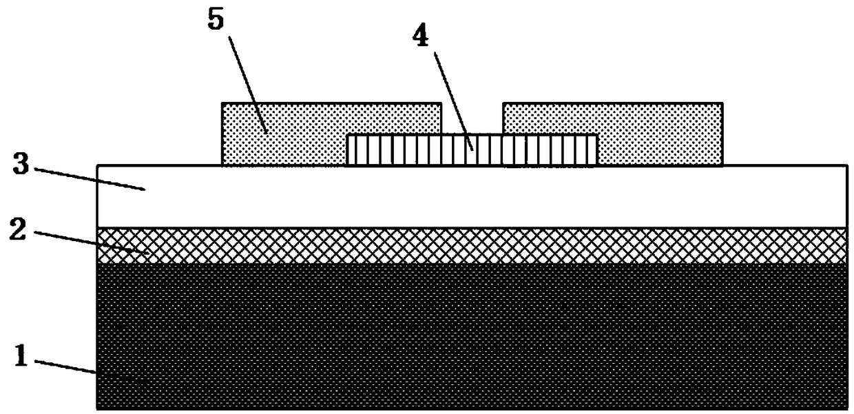
[0022] A two-dimensional material photodetector with embedded mirrors, such as figure 1 As shown, a substrate 1 , a metal mirror 2 , a dielectric layer 3 , a two-dimensional material 4 , and a source-drain electrode 5 are sequentially included from bottom to top.

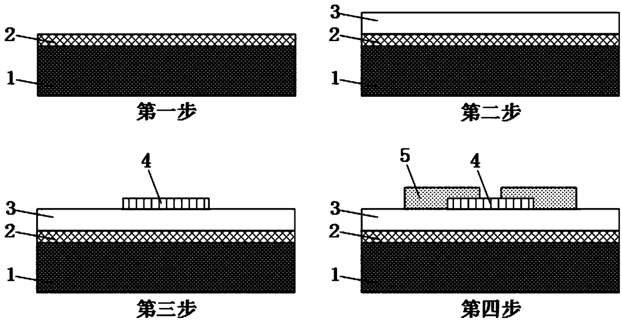
[0023] like figure 2 As shown, the preparation method of the above-mentioned two-dimensional material photodetector with built-in reflector comprises the following steps:

[0024] In the first step, a metal mirror 2 with high reflectivity is plated on the substrate 1; wherein, the material used for the substrate 1 is silicon, and the material used for the metal mirror 2 is silver.

[0025] In the second step, a dielectric layer 3 is plated on the metal reflector 2; wherein, the material used for the dielectric layer 3 is zirconium dioxide.

[0026] In the third step, the two-dimensional material 4 is grown on the dielectric layer 3 by chemical vapor deposition; wherein, the material used for the two-dimensional m...

Embodiment 2

[0029] A two-dimensional material photodetector with embedded mirrors, such as figure 1 As shown, a substrate 1 , a metal mirror 2 , a dielectric layer 3 , a two-dimensional material 4 , and a source-drain electrode 5 are sequentially included from bottom to top.

[0030] like figure 2 As shown, the preparation method of the above-mentioned two-dimensional material photodetector with built-in reflector comprises the following steps:

[0031] In the first step, a metal mirror 2 with high reflectivity is coated on the substrate 1; wherein, the material used for the substrate 1 is germanium, and the material used for the metal mirror 2 is aluminum.

[0032] In the second step, a dielectric layer 3 is plated on the metal reflector 2; wherein, the material used for the dielectric layer 3 is hafnium dioxide.

[0033] The third step is to grow the two-dimensional material 4 on the dielectric layer 3 by chemical vapor deposition; wherein, the material used for the two-dimensional m...

Embodiment 3

[0036] A two-dimensional material photodetector with embedded mirrors, such as figure 1 As shown, a substrate 1 , a metal mirror 2 , a dielectric layer 3 , a two-dimensional material 4 , and a source-drain electrode 5 are sequentially included from bottom to top.

[0037] like figure 2 As shown, the preparation method of the above-mentioned two-dimensional material photodetector with built-in reflector comprises the following steps:

[0038] In the first step, a metal mirror 2 with high reflectivity is coated on the substrate 1; wherein, the material used for the substrate 1 is germanium, and the material used for the metal mirror 2 is aluminum.

[0039] In the second step, a dielectric layer 3 is plated on the metal reflector 2; wherein, the material used for the dielectric layer 3 is hafnium dioxide.

[0040] In the third step, the two-dimensional material 4 is grown on the dielectric layer 3 by using a micromechanical lift-off method; wherein, the material used for the t...


PUM


Abstract

The invention belongs to the technical field of micronano photoelectronics, and discloses a two-dimensional material photoelectric detector with an embedded reflecting mirror and a fabrication methodthereof. The two-dimensional material photoelectric detector sequentially comprises a substrate, a metal reflecting mirror, a dielectric layer, a two-dimensional material and a source-drain electrodefrom bottom to top, wherein the metal reflecting mirror is embedded between the substrate and the dielectric layer. The fabrication method comprises the steps of plating a layer of high-reflectivity metal on the substrate; plating the dielectric layer on the metal reflecting mirror; growing or transferring the two-dimensional material onto the dielectric layer; and plating the source-drain electrode on the two-dimensional material. The fabrication method of the two-dimensional material photoelectric detector with the embedded reflecting mirror has the advantages of a few process steps, high efficiency and the like and is simple to operate, and the detection performance of the device is effectively improved.

Description

technical field [0001] The invention belongs to the technical field of micro-nano optoelectronics, and more specifically relates to a two-dimensional material photodetector with built-in reflectors and its preparation method and application. Background technique [0002] It has only been a few years since the new two-dimensional materials really came into people's attention, and it has quickly become a hot topic in the field of materials in the world, with new discoveries and new breakthroughs constantly emerging. Two-dimensional materials usually have a certain band gap and unique mechanical, optical, and electrical properties, and gradually become an emerging two-dimensional material system, and the research on two-dimensional material photodetectors is also increasingly prosperous. However, the area of ​​two-dimensional materials is usually relatively small, the thickness is also very thin, and they are translucent. Therefore, their light absorption efficiency is relative...

Claims


Application Information

Patent Timeline
Patent Type & Authority Applications(China)
IPC IPC(8): H01L31/0232H01L31/08H01L31/18
CPCH01L31/02327H01L31/08H01L31/18Y02P70/50
Inventor 杨亿斌李京波招瑜肖也罗东向牟中飞郑照强
Owner GUANGDONG UNIV OF TECH
Why Eureka
Try Eureka