Transferring method of edge-free vertical structure LED chip substrate

A LED chip and vertical structure technology, applied in the direction of electrical components, circuits, semiconductor devices, etc., can solve the problems of easy warping, high cost, high stress, etc., to prevent lateral immersion, prevent scratches, and improve efficiency Effect

Active Publication Date: 2018-11-23
HEYUAN CHOICORE PHOTOELECTRIC TECH CO LTD
View PDF8 Cites 4 Cited by
  • Summary
  • Abstract
  • Description
  • Claims
  • Application Information

AI Technical Summary

Problems solved by technology

Dry etching has high precision but slow speed and high cost; wet etching has low cost but strong anisotropy and uncontrollable corrosion effect; electroplated metal substrate has low cost but high stress and is prone to warping; and bonding High cost of metal and bonding equipment

Method used


Image

  • Transferring method of edge-free vertical structure LED chip substrate
  • Transferring method of edge-free vertical structure LED chip substrate
  • Transferring method of edge-free vertical structure LED chip substrate

Examples


Embodiment 1

[0056] refer to Figure 1-6 , a method for transferring an edgeless vertical structure LED chip substrate, comprising,

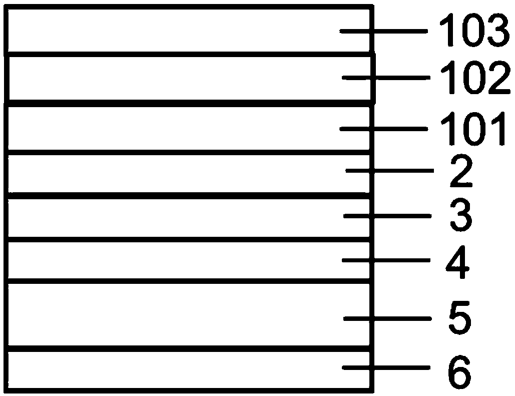
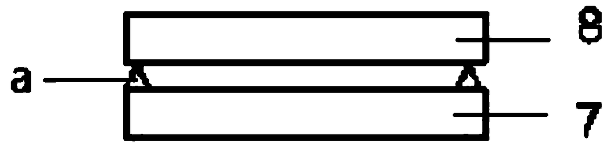
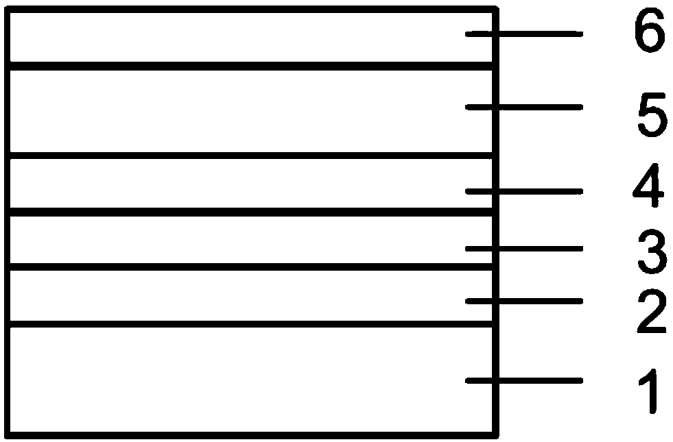
[0057] Step of depositing metal layer: first obtain silicon-based LED epitaxial wafer 1, deposit metal layer on silicon-based LED epitaxial wafer 1, metal layer includes reflector layer 2, reflector protection layer 3 and bonding layer metal 4, reflector layer 2 E-beam is used to deposit on the surface of the silicon-based LED epitaxial wafer 1 (non-silicon substrate surface), the mirror protective layer 3 is deposited on the surface of the reflective mirror layer 2, and the bonding layer metal 4 is deposited on the surface of the reflective mirror protective layer 3 to obtain an epitaxial wafer 7. The silicon-based LED epitaxial wafer 1 includes an epitaxial layer 101, a residual silicon layer 102 removed by a wet method, and a residual silicon layer 103 removed by a dry method;

[0058] The mirror layer 2 is an Ag-based stacked mirror with a structure of ...

Embodiment 2

[0066] A method for transferring a vertical structure LED chip substrate without loss of edges, comprising,

[0067] Depositing metal layer steps: first obtain the silicon-based LED epitaxial wafer, deposit the metal layer on the silicon-based LED epitaxial wafer, the metal layer includes the reflector layer, the reflector protection layer and the bonding layer metal, and the reflector layer is deposited on the silicon-based LED epitaxial wafer surface, the mirror protective layer is deposited on the surface of the mirror layer, and the bonding layer metal is deposited on the surface of the mirror protective layer to obtain an epitaxial wafer; the mirror layer is TiO 2 / SiN x Distributed Bragg reflector, the structure of Bragg reflector is TiO 2 and SiN x Alternately arranged into a periodic structure film in the form of ABAB, prepared by DBR electron beam evaporation station, with TiO 2 and SiN x as one cycle, a total of 17 cycles, each layer of TiO 2 The thickness is 12...

Embodiment 3

[0075] A method for transferring a vertical structure LED chip substrate without loss of edges, comprising,

[0076] Deposit metal layer steps: first obtain silicon-based LED epitaxial wafer, deposit metal layer on silicon-based LED epitaxial wafer, metal layer includes mirror layer, mirror protection layer and bonding layer metal, mirror layer is deposited on silicon by E-beam Based on the surface of the LED epitaxial wafer, the mirror protective layer is deposited on the surface of the mirror layer, and the bonding layer metal is deposited on the surface of the mirror protective layer to obtain the epitaxial wafer; the mirror layer is an Ag-based laminated mirror, and its structure is Pd / Ag / W / Au, the thickness is 2 / 200 / 800 / 200nm; the mirror protective layer is TiW / Pt laminated layer, the laminated period is 5, and the thickness of one laminated period of the mirror protective layer is 300 / 200nm; The bonding layer metal is In / Sn, and the thickness of the bonding layer metal ...


PUM


Abstract

The invention discloses a transferring method of an edge-free vertical structure LED chip substrate. The transferring method of the edge-free vertical structure LED chip substrate comprises a metal layer depositing step, an epitaxial wafer surface treatment step, a substrate deposition transferring step, a bonding step, a thinning step, a residual silicon removal step, and a vertical LED chip preparation step. The transferring method of the edge-free vertical structure LED chip substrate disclosed by the invention can solve the problems in the current substrate transferring process by means ofthe epitaxial wafer surface treatment step, the thinning step, the residual silicon removal step and the like, which can obtain a comparatively excellent substrate transferring technology.

Description

technical field [0001] The invention relates to the field of LED manufacturing, in particular to a method for transferring a vertical structure LED chip substrate with no edge damage. Background technique [0002] At present, sapphire-based horizontal structure LED chips cannot be applied to the field of high-power LED lighting due to poor heat dissipation, electrode light blocking, and lateral current congestion effects; the corresponding vertical structure LED chips are excellent due to their single-sided light emission and vertical current distribution. , Excellent heat dissipation and other characteristics gradually replace horizontal structure LED chips in the field of high-power lighting. Substrate transfer is the core technology of vertical structure LED chips. Since the growth substrate is generally sapphire or silicon, the sapphire substrate is not conductive and needs to be removed by laser lift-off (LLO). At the same time, since the bandgap material of silicon is...

Claims


Application Information

Patent Timeline
Patent Type & Authority Applications(China)
IPC IPC(8): H01L33/00H01L33/62
CPCH01L33/005H01L33/62
Inventor 李国强
Owner HEYUAN CHOICORE PHOTOELECTRIC TECH CO LTD
Why Eureka
Try Eureka