A light-emitting diode epitaxial wafer and its manufacturing method

A technology of light-emitting diodes and manufacturing methods, which is applied in the direction of semiconductor devices, electrical components, circuits, etc., can solve the problems of reducing the combined luminous efficiency of electrons and holes, reducing the luminous efficiency of light-emitting diodes, and dislocation of corresponding positions, so as to improve the luminous Efficiency, impact reduction, and the effect of reducing the degree of distortion

Active Publication Date: 2019-10-08
HC SEMITEK ZHEJIANG CO LTD
View PDF12 Cites 1 Cited by
  • Summary
  • Abstract
  • Description
  • Claims
  • Application Information

AI Technical Summary

Problems solved by technology

[0005] Since the concentration of In in the InGaN well layer remains unchanged, the growth temperature also remains unchanged, which means that In is doped into the GaN lattice at one time, and the energy band of the GaN lattice will be greatly affected during the process of absorbing In. The impact is thus tilted, resulting in energy band distortion, which will cause the dislocation of the corresponding positions of electrons and holes in the InGaN well layer, resulting in fewer overlapping areas between electron wave functions and hole wave functions, reducing the electron and hole wave function. The radiative recombination luminous efficiency of the hole, thereby reducing the luminous efficiency of the light-emitting diode

Method used


Image

  • A light-emitting diode epitaxial wafer and its manufacturing method
  • A light-emitting diode epitaxial wafer and its manufacturing method

Examples


Embodiment 1

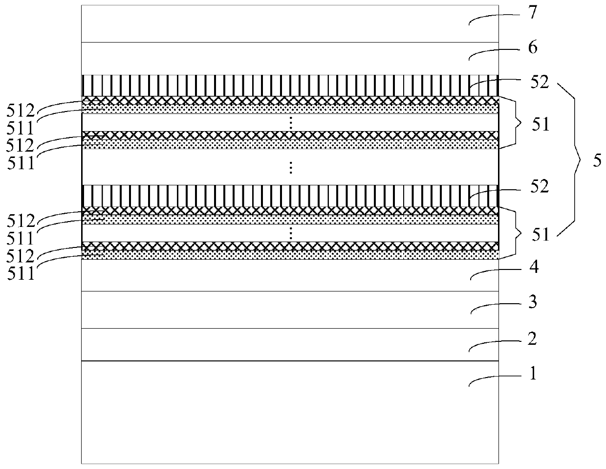
[0029] An embodiment of the present invention provides a light emitting diode epitaxial wafer, figure 1 It is a schematic structural diagram of a light-emitting diode epitaxial wafer provided by an embodiment of the present invention, as shown in figure 1 As shown, the light-emitting diode epitaxial wafer includes a substrate 1, a buffer layer 2, an undoped GaN layer 3, an N-type layer 4, an active layer 5, an electron blocking layer 6, and a P-type layer stacked on the substrate 1 in sequence. Layer 7, the active layer 5 includes a plurality of well layers 51 and barrier layers 52 alternately grown in a plurality of periods.

[0030] Each well layer 51 is a superlattice structure composed of the first sublayer 511 and the second sublayer 512, the first sublayer 511 and the second sublayer 512 are both InGaN layers, and the In in the first sublayer 511 The concentration is greater than that of In in the second sublayer 512 .

[0031] Each well layer in the active layer of th...

Embodiment 2

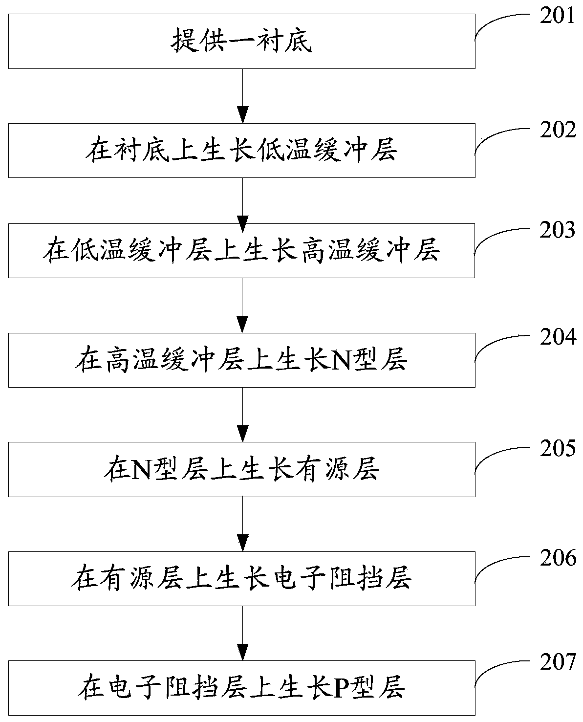
[0048] An embodiment of the present invention provides a method for manufacturing a light-emitting diode epitaxial wafer, which is used to manufacture the light-emitting diode epitaxial wafer provided in Embodiment 1, figure 2 It is a method flowchart of a method for manufacturing a light-emitting diode epitaxial wafer provided by an embodiment of the present invention, as shown in figure 2 As shown, the manufacturing method includes:

[0049] Step 201, providing a substrate.

[0050] Optionally, the substrate is sapphire.

[0051] Specifically, this step 201 includes:

[0052] Under a hydrogen atmosphere, treat the substrate at high temperature for 5-6 minutes. Wherein, the temperature of the reaction chamber is 1000-1100° C., and the pressure of the reaction chamber is controlled at 200-500 torr.

[0053] Step 202, growing a low-temperature buffer layer on the substrate.

[0054] In this embodiment, Veeco K465i or C4MOCVD (Metal Organic Chemical Vapor Deposition, Meta...


PUM


Abstract

The invention discloses a light-emitting diode epitaxial wafer and a manufacturing method thereof, and belongs to the technical field of semiconductors. An active layer of the light-emitting diode epitaxial wafer comprises a plurality of well layers and barrier layers which are periodically and alternatively grown, wherein each well layer is a superlattice structure comprising a first sub-layer and a second sub-layer, the first sub-layer and the second sub-layer both are InGaN layers, the In concentration in the first sub-layer is larger than the In concentration in the second sub-layer, and In of each well layer is gradually doped to GaN lattices. Compared with the prior art which the In of the InGaN well layers is doped into the GaN lattices in one time, the impact of the In doping to anenergy band can be reduced, so that the distortion degree of the energy band is reduced, the overlap region of an electron wave function and a hole wave function is expanded, the electron and hole radiation combination light-emitting efficiency is improved, and the light-emitting efficiency of a light-emitting diode is further improved.

Description

technical field [0001] The invention relates to the technical field of semiconductors, in particular to a light-emitting diode epitaxial wafer and a manufacturing method thereof. Background technique [0002] LED (Light Emitting Diode, Light Emitting Diode) is a semiconductor electronic component that can emit light. As an efficient, environmentally friendly and green new solid-state lighting source, it is being rapidly and widely used, such as traffic lights, car interior and exterior lights, urban landscape lighting, mobile phone backlights, etc. [0003] The epitaxial wafer is the main component of the LED. The existing LED epitaxial wafer includes a substrate and a low-temperature buffer layer, a high-temperature buffer layer, an N-type layer, an active layer, an electron blocking layer, and a P-type layer stacked on the substrate in sequence. . Wherein, the active layer includes InGaN well layers and barrier layers alternately grown in multiple periods, and the concen...

Claims


Application Information

Patent Timeline
Patent Type & Authority Patents(China)
IPC IPC(8): H01L33/00H01L33/04H01L33/32
Inventor 姚振从颖胡加辉李鹏
Owner HC SEMITEK ZHEJIANG CO LTD
Why Eureka
Try Eureka