Gold plating method for gold fingers and gold finger circuit board

A golden finger and circuit board technology, applied in printed circuit, printed circuit manufacturing, printed circuit components, etc., can solve problems such as rising material costs, inability to completely remove, product scratches, etc., to reduce product production difficulty and production costs , Avoid the possibility of gold plating on the copper surface, reduce the effect of material cost input

Inactive Publication Date: 2018-11-23
PEKING UNIV FOUNDER GRP CO LTD +1
View PDF3 Cites 6 Cited by
  • Summary
  • Abstract
  • Description
  • Claims
  • Application Information

AI Technical Summary

Problems solved by technology

[0005] (1) High precision is required for pattern transfer alignment, and it is prone to seepage of gold at the bottom of the gold finger electroplating lead and cannot be completely removed;
[0006] (2) After gold-plating, do solder mask and gold-melt, and the gold-plated gold fingers are easy to scratch, which affects the appearance yield;
[0007] (3) Gold plating is done after gold plating, the dry film has poor film release during the gold plating process, and the gold finger plating leads are gold-plated again, which will cause an increase in material costs;
[0008] (4) Since the gold finger electroplating lead extends to the edge of the board, it is easy to pull up the bottom copper skin during molding and cause burrs around the gold surface. If it is not removed, it will cause scratches between products during handling. Alkaline etching is required to remove burrs. One more production process

Method used


Image

  • Gold plating method for gold fingers and gold finger circuit board
  • Gold plating method for gold fingers and gold finger circuit board
  • Gold plating method for gold fingers and gold finger circuit board

Examples


Embodiment Construction

[0031] The following will clearly and completely describe the technical solutions in the embodiments of the present invention with reference to the accompanying drawings in the embodiments of the present invention. Obviously, the described embodiments are only some, not all, embodiments of the present invention. Based on the embodiments of the present invention, all other embodiments obtained by persons of ordinary skill in the art without making creative efforts belong to the protection scope of the present invention.

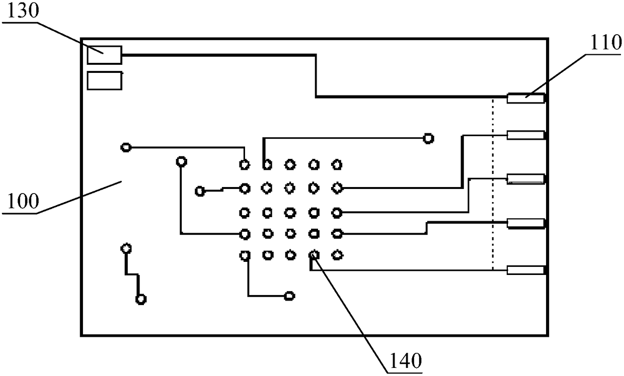
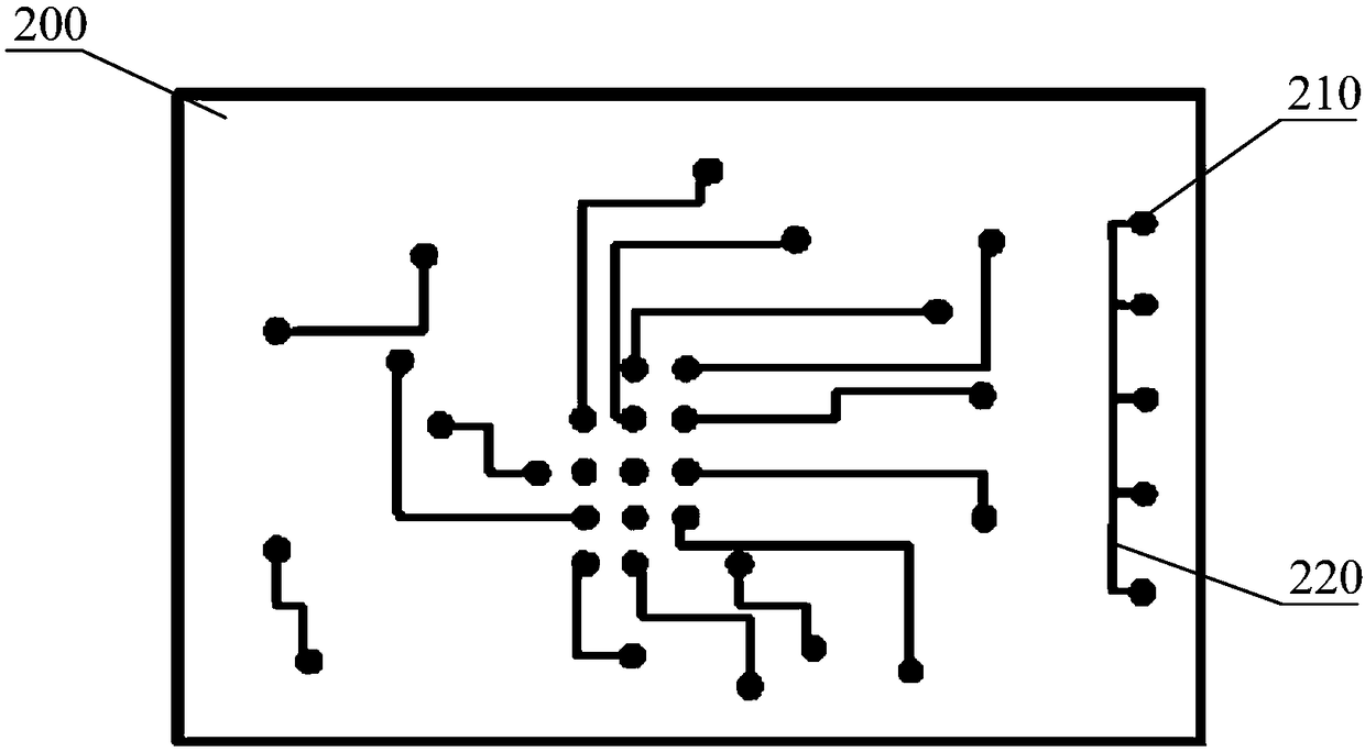
[0032] figure 1 The flow chart of the gold plating method for gold fingers provided by the embodiment of the present invention. Such as figure 1 As shown, the present embodiment provides a method for gold-plated gold fingers, and the specific steps of the method are as follows:

[0033] S101 , covering the non-gold-plated area on the outer layer circuit board 100 with a dry film, so that the gold-plated area of ​​the gold finger 110 is exposed.

[0034] Suc...


PUM


Abstract

The invention provides a gold plating method for gold fingers and a gold finger circuit board. According to the gold plating method, a secondary outer pad is arranged corresponding to a projection position of each gold finger on an outer circuit board on a secondary outer circuit board; each secondary outer pad is electrically connected by adopting an electroplated lead; first blind holes are formed in each gold finger and are filled up through hole-filling electroplating, thereby conducting each gold finger and the corresponding secondary outer pad; the gold fingers are connected with a powersupply for carrying out gold plating; and the electroplated lead connected with each secondary outer pad is finally disconnected through depth-controlled drilling, so that each gold finger is broken,thereby achieving production of the gold fingers free of the electroplated lead on the surfaces. A gold-plated lead is arranged on the secondary outer circuit board and the electroplated lead is notdesigned on the surface of the outer circuit board, so that the scratch probability of the gold fingers in the production process is reduced, the quality of a product is improved, the material cost isreduced, gold permeating on a copper surface is avoided, the dependence on manual repair in the production process is reduced and the defect caused by the electroplated lead on the outer circuit board in the prior art is avoided.

Description

technical field [0001] The invention relates to the field of circuit boards, in particular to a gold-finger gold-plating method and a gold-finger circuit board. Background technique [0002] In order to meet the development requirements of diversification and portability of electronic products, printed circuit boards not only have high aperture ratio and high-precision features of fine lines, but also high-density circuit board designs such as golden fingers for high-speed communication. In the functional application of electronic products, in order to reduce the loss of signal transmission, high-speed storage products generally need to use circuit boards with gold finger design as the carrier board. Gold finger is composed of many golden-yellow conductive contacts, its surface is plated with anti-oxidation and highly conductive gold, and the conductive contacts are arranged like fingers, so it is called "gold finger". [0003] The commonly used gold fingers are usually des...

Claims


Application Information

Patent Timeline
Patent Type & Authority Applications(China)
IPC IPC(8): H05K3/40H05K3/24H05K1/11
CPCH05K3/403H05K1/117H05K3/241H05K2203/0723
Inventor 金立奎车世民陈德福王世威徐竟成
Owner PEKING UNIV FOUNDER GRP CO LTD
Why Eureka
Try Eureka