
Photo-curing printing-based microfluid chip and manufacturing method thereof

A microfluidic chip, light curing technology, applied in the fields of biochemical equipment and methods, biochemical instruments, tissue cell/virus culture devices, etc. High-level requirements, to achieve the effect of strong customizability, flexible micro-machining process design, and simple process

Pending Publication Date: 2018-11-27
HANGZHOU DIANZI UNIV
View PDF0 Cites 4 Cited by
  • Summary
  • Abstract
  • Description
  • Claims
  • Application Information

AI Technical Summary

Problems solved by technology

This process needs to be completed in a clean room. The preparation technology is difficult, the operation technology is high, the preparation cycle is long, and the equipment is expensive, which seriously restricts its large-scale production and application, and also restricts the flexibility of chip design.

Method used


Image

  • Photo-curing printing-based microfluid chip and manufacturing method thereof
  • Photo-curing printing-based microfluid chip and manufacturing method thereof
  • Photo-curing printing-based microfluid chip and manufacturing method thereof

Examples


Embodiment Construction

[0034] The present invention will be further described below in conjunction with accompanying drawing.

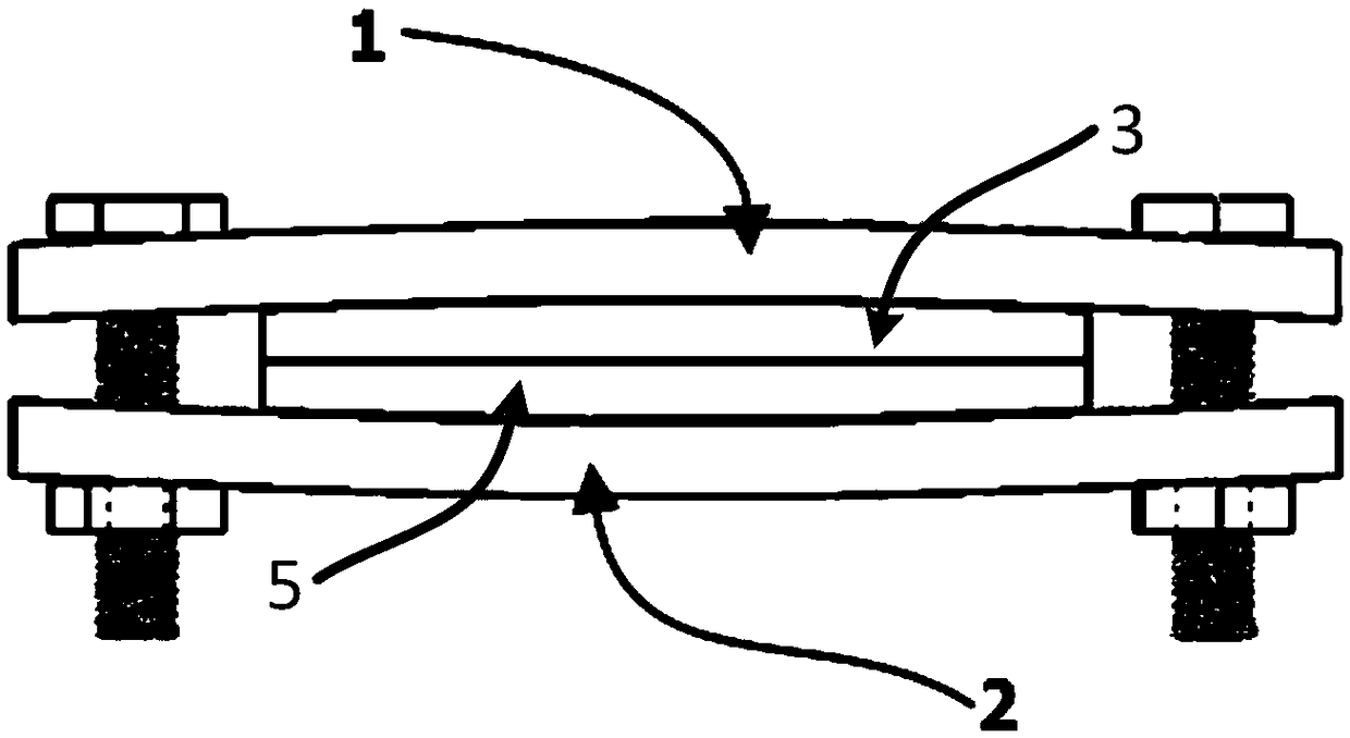
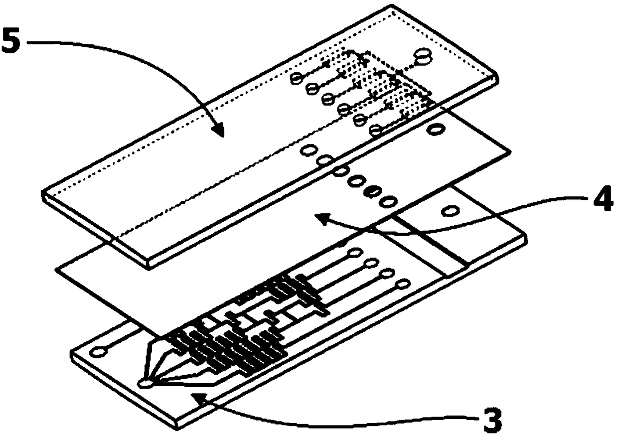
[0035] Such as figure 1 and 2 As shown, the microfluidic chip based on photocuring printing includes a top plate 1, a bottom plate 2 and a chip body. The main body of the chip is composed of a concentration gradient chip 3 , a bonding film 4 and a cell culture chip 5 stacked in sequence. The materials of the top plate 1 and the bottom plate 2 are organic glass. The concentration gradient chip 3 and the cell culture chip 5 are made of transparent photosensitive resin. The bonding film 4 is made of dimethylsiloxane (PDMS). The thickness of the bonding film 4 is 200um. The outer surfaces of the concentration gradient chip 3 and the cell culture chip 5 are both convex arc shapes. The distance between the most convex part of the outer surface of the concentration gradient chip 3 and the cell culture chip 5 and the edges on both sides along the thickness direction of the co...


PUM


Abstract

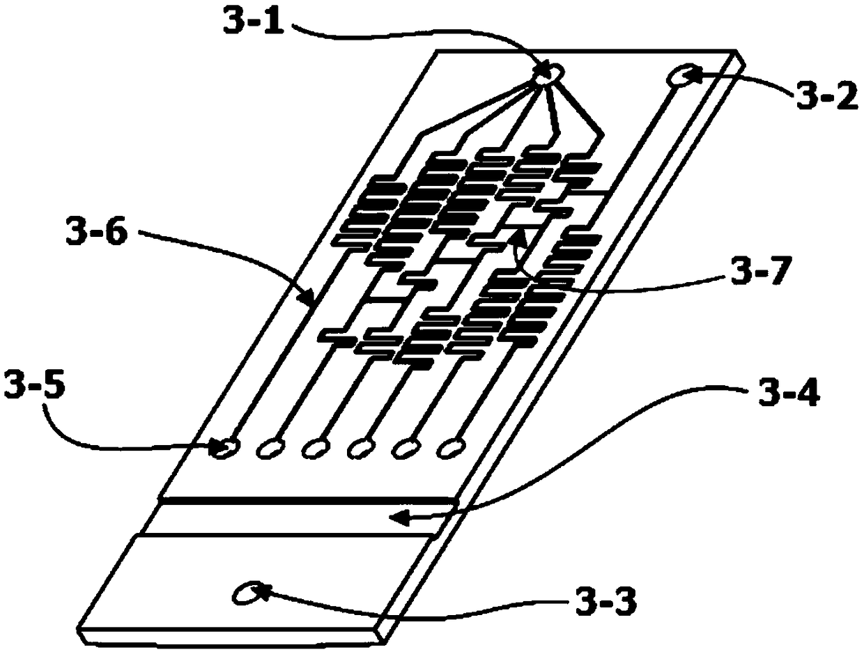
The invention discloses a photo-curing printing-based microfluid chip and a manufacturing method thereof. An existing microfluid chip is great in preparation technology, high in demand on operating technology, long in preparation period and expensive in equipment. The photo-curing printing-based microfluid chip comprises a top plate, a bottom plate and a chip main body. The chip main body is composed of a concentration gradient chip, a bonding film and a cell culture chip which are overlaid successively. The outer side faces of the concentration gradient chip and the cell culture chip are in protruding arc shape. A buffer liquid hole, a nutrient liquid hole, a first liquid outlet hole, a resistor disc placing groove, n liquid storage holes, n zigzag runners and (n-2) connecting runners arearranged on the inner side face of the concentration gradient chip, wherein n is greater than or equal to 2 but less than or equal to 10. A first liquid through hole and n second through holes are formed in the bonding film. By means of a bonding mode of a blooming extrusion manner, the leakage problem when a photosensitive resin chip is combined is solved.

Description

technical field [0001] The invention belongs to the technical field of microfluidic chips, and in particular relates to a modular concentration gradient microfluidic chip based on photocuring printing and a manufacturing method thereof. Background technique [0002] Microfluidic chips have good optical properties, colorless, transparent, non-toxic, cheap, durable, and have certain advantages such as chemical inertness and light transmission. They are widely used in biomedicine, environmental testing, food safety, material preparation and other fields. application. The existing microfluidic chip preparation process usually adopts the idea of ​​preparing the mold first, and then pouring the mold. The microfluidic mold is manufactured through complex processes such as mask plate preparation, glue removal, photolithography, and development, and then poured with different materials. Molding and demoulding to obtain the required chip substrate. This process needs to be completed...

Claims


Application Information

Patent Timeline
IPC IPC(8): C12M3/00
CPCC12M23/16C12M23/20C12M29/00C12M41/22
Inventor 刘海强蔡越龚友平陈国金
Owner HANGZHOU DIANZI UNIV
Learn More