
Method for making double-sided wire-buried printed circuit board by using imageable dielectric material

A technology for printed circuit boards and dielectric materials, applied in the directions of printed circuits, printed circuit manufacturing, multilayer circuit manufacturing, etc., can solve problems such as poor alignment of buried layers, open circuits, etc. Positioning system system, the effect of improving product quality

Inactive Publication Date: 2018-11-27
SHANGHAI MEADVILLE SCI & TECH
View PDF5 Cites 1 Cited by
  • Summary
  • Abstract
  • Description
  • Claims
  • Application Information

AI Technical Summary

Problems solved by technology

[0004] The purpose of the present invention is to provide a method for making double-sided embedding printed circuit boards with imageable dielectric materials, which can solve the problem of poor alignment between embedding layers, and at the same time avoid the problem of open circuit caused by excessive copper reduction, which can be more Better guarantee the quality of double-sided embedding printed circuit boards

Method used


Image

  • Method for making double-sided wire-buried printed circuit board by using imageable dielectric material
  • Method for making double-sided wire-buried printed circuit board by using imageable dielectric material
  • Method for making double-sided wire-buried printed circuit board by using imageable dielectric material

Examples


Embodiment Construction

[0036] see Figure 1 to Figure 9 , the method for making a double-sided embedding printed circuit board made of an imageable dielectric material according to the present invention, which comprises the following steps:

[0037] a) First provide a core board 100 with a detachable structure, 101 is a detachable carrier copper foil, and 102 is an auxiliary copper foil for forming the first circuit pattern, such as figure 1 shown;

[0038] b) On the surface of the auxiliary copper foil 102, the first circuit pattern 1021 of the printed board is made by pattern transfer and pattern electroplating, and the positioning reference pattern 1022 is made at the same time, such as figure 2 shown;

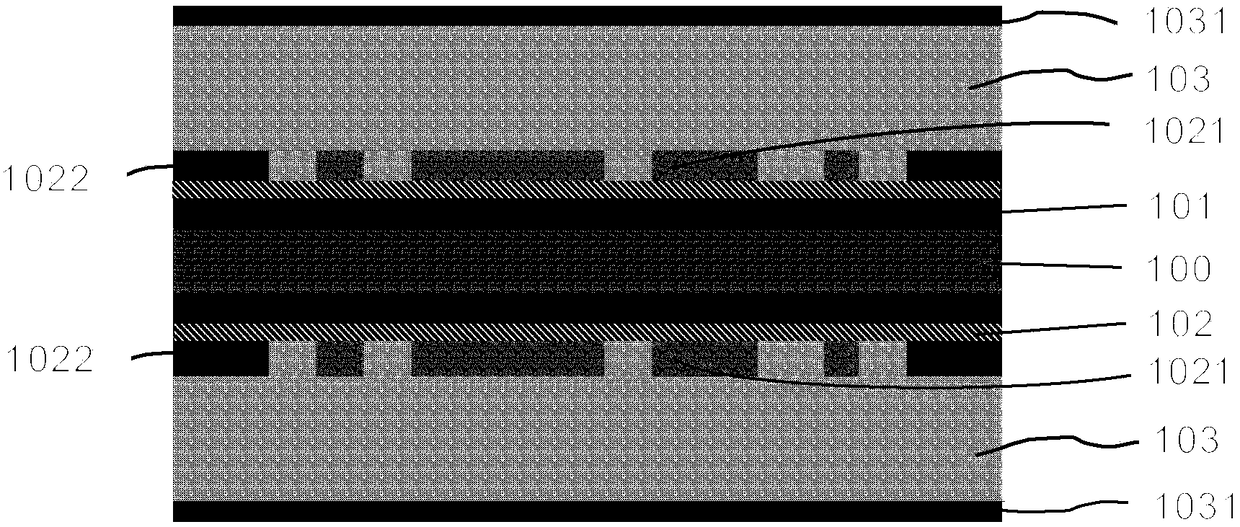
[0039] c) On the first circuit pattern 1021, an imageable dielectric material 103 is pressed to form a first embedded circuit, 1021 is the first embedded circuit, and 1031 is an imageable dielectric material protective layer, such as image 3 shown;

[0040] d) Use the positioning reference...


PUM


Abstract

The invention relates to a method for making a double-sided wire-buried printed circuit board by using an imageable dielectric material. The method comprises the following steps: (a) firstly, providing a detachable core board, and arranging a carrier copper foil and an auxiliary copper foil on the surface of the core board; (b) making a first line pattern on the surface of the auxiliary copper foil; (c) laminating the imageable dielectric material on the first line pattern to form a first buried line; (d) locating by using the first line pattern to form a sinking type line slot and a counterbore with a certain depth; (e) locating by using the first line pattern, and processing counterbore again with laser so as to make a complete through hole; (f) carrying out copper plating on the imageable dielectric material, and fully filling the sinking type line slot and the through hole with copper; (g) removing the plated copper on the surface of the imageable dielectric material to form a second buried line; (h) disassembling the detachable core plate to remove the auxiliary copper foil on the surface of the first line pattern; (i) forming a solder mask on the surface of the circuit boardand carrying out surface treatment to obtain the double-sided wire-buried printed circuit board.

Description

technical field [0001] The invention relates to the manufacturing technology of printed circuit boards or semiconductor integrated circuit packaging substrates, in particular to a method for making double-sided embedding printed circuit boards with imageable dielectric materials. Background technique [0002] With the continuous advancement of science and technology, the electronics industry has developed rapidly, and electronic products have already entered the stage of functional and intelligent development. In order to better meet the needs of high integration and miniaturization of electronic products, printed circuit boards or semiconductor integration On the premise of ensuring good electrical and thermal properties of electronic products, circuit packaging substrates are also developing in the direction of lightness, thinness, shortness and smallness. [0003] Because the design of printed circuit boards or semiconductor integrated circuit packaging substrates is gett...

Claims


Application Information

Patent Timeline
Patent Type & Authority Applications(China)
IPC IPC(8): H05K3/46H05K3/10
CPCH05K3/107H05K3/4644
Inventor 徐友福
Owner SHANGHAI MEADVILLE SCI & TECH
Learn More