

A stacked SRAM array structure with high energy efficiency and low power consumption
A technology of array structure and utilization rate, which is applied in the field of stacked SRAM array structure, can solve the problems of high conduction loss energy utilization efficiency of converters, low voltage conversion ratio, etc., and achieve the goals of easy implementation, avoiding design, and avoiding voltage loss Effect
Active Publication Date: 2018-12-07
XI AN JIAOTONG UNIV
View PDF7 Cites 0 Cited by
- Summary
- Abstract
- Description
- Claims
- Application Information
AI Technical Summary
Problems solved by technology
In the method of reducing the power supply voltage, a linear regulator or a step-down DC converter can be used, but the voltage conversion ratio (that is, the ratio of the output voltage to the input voltage) of this structure is very low, and due to the high conduction of the converter Loss and low output power, its energy utilization efficiency also becomes low
Method used
View moreImage
Smart ImageViewing Examples

Examples
Embodiment 1
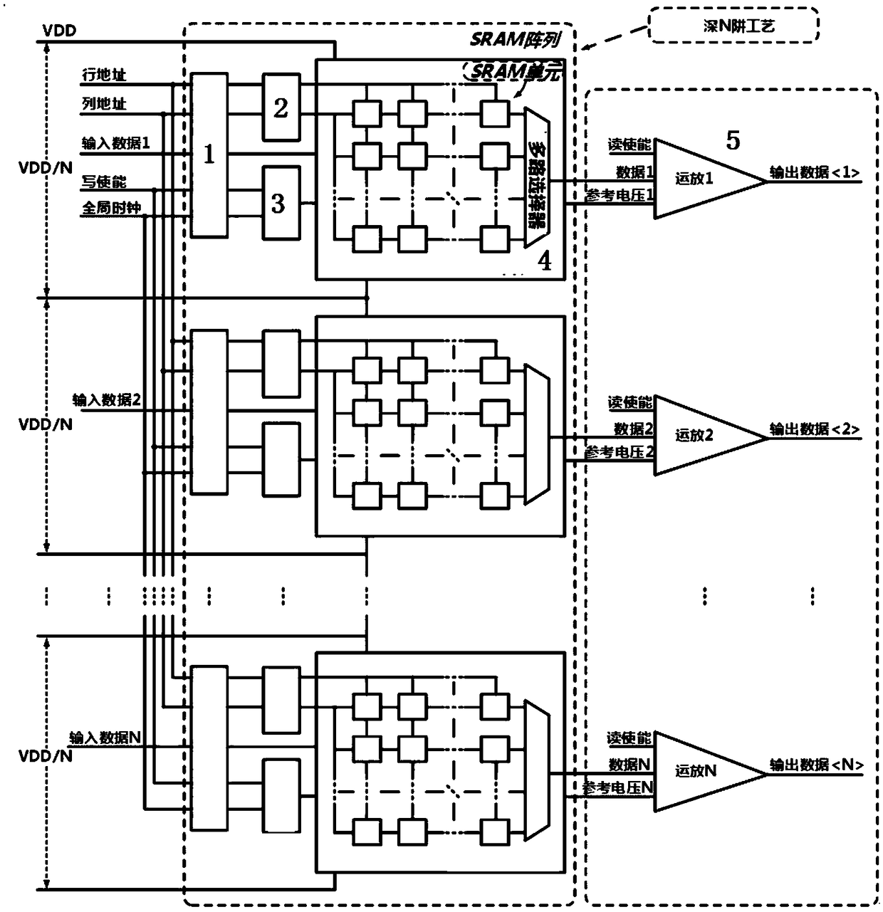
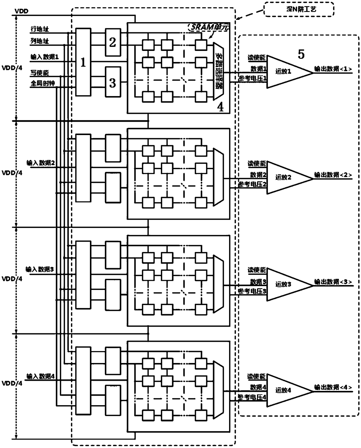
[0033] Suppose the battery voltage of the stacked SRAM is 1.8V, the write enable signal is a square wave signal with a frequency of 10kHz, and the global clock signal is a square wave signal with a frequency of 20kHz. Stable at 1.8V, 1.35V, 0.9V, and 0.45V. At the same time, in the case of a voltage range of 450mV, the write / read power consumption of an SRAM cell is only 2.45pJ / acc and 2.18pJ / acc for each access, and the highest output power consumption is only 60μW. The deviation of power consumption is within 10%, and the efficiency in the worst case is as high as 94%, so as to achieve the purpose of low power consumption and high energy conversion efficiency.
Login to View More PUM
 Abstract
The invention discloses a stacked SRAM array structure with high energy utilization rate and low power consumption, the structure being formed by N layers of SRAM circuits. The high voltage of the i SRAM circuit is shown in the description and the low voltage of the i SRAM circuit is shown in the description , wherein 1<=i<=N, N is greater than or equal to 1, and i and N are all positive integers. The power consumption of the SRAM array structure is low and the energy utilization ratio is high.
Description
technical field [0001] The invention belongs to the technical field of integrated circuits and relates to a stacked SRAM array structure with high energy utilization rate and low power consumption. Background technique [0002] SRAM is currently widely used in various fields. We represent a bit of binary information by the different stable states it is in. When there is no external signal, the flip-flop can maintain a certain stable state for a long time, so it is also called a static memory. Due to the vigorous development of implantable and wearable devices, smart mobile terminals represented by operating systems such as Android have higher and higher requirements for processors. At the same time, the capacity of batteries is growing very slowly. , the demand for high energy utilization and low power consumption becomes more and more frequent. Static random access memory (SRAM) is one of the important components, and SRAM with low power consumption and high energy effic...
Claims
Login to View More Application Information
Patent Timeline
 IPC IPC(8): G11C11/4074
CPCG11C11/4074
Inventor范世全董军赵洋张芮苟伟耿莉
OwnerXI AN JIAOTONG UNIV