Super-wide incidence angle microwave absorbing materials and a production method thereof

A wave absorbing material, incident angle technology, applied in conductive coatings, coatings, electrical components, etc., can solve the problems of increasing operation difficulty and platform cost, and achieve the effects of low cost, reduced storage space, and environmental protection of products

Inactive Publication Date: 2018-12-07
西安安聚德纳米科技有限公司
View PDF4 Cites 12 Cited by
  • Summary
  • Abstract
  • Description
  • Claims
  • Application Information

AI Technical Summary

Problems solved by technology

For example, in the field antenna performance test, surface traveling waves and reflections need to be removed. Otherwise, high antenna and test platform locations must be used, which increases the difficulty of operation and the cost of the platform. Both surface traveling waves and surface reflections require high incident angle absorbing materials.

Method used


Image

  • Super-wide incidence angle microwave absorbing materials and a production method thereof
  • Super-wide incidence angle microwave absorbing materials and a production method thereof
  • Super-wide incidence angle microwave absorbing materials and a production method thereof

Examples


Embodiment 1

[0047] Example 1: Long-term use of wave-absorbing honeycomb with a height of 140 mm and a temperature of 180 °C

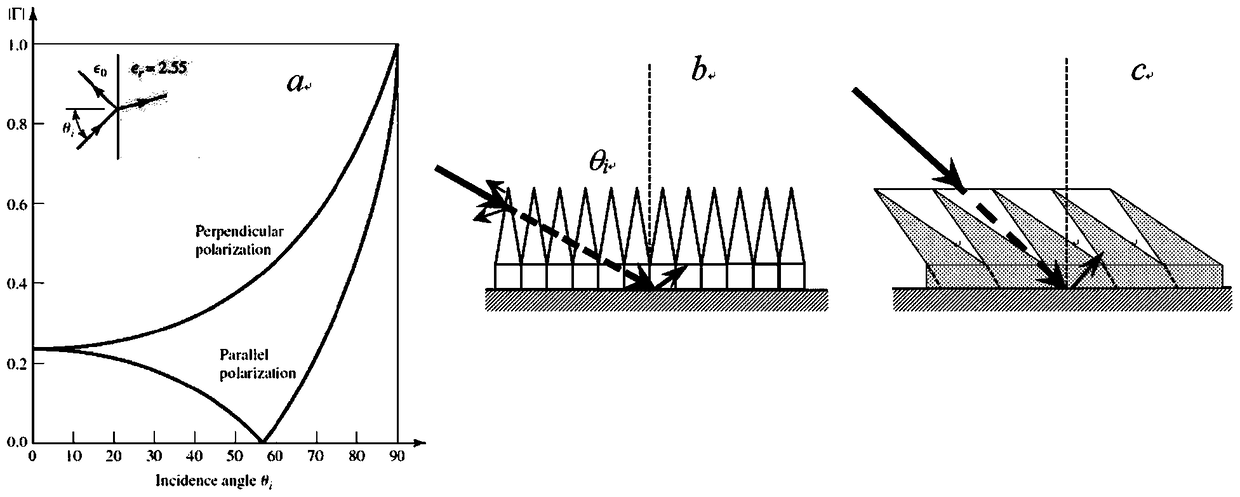
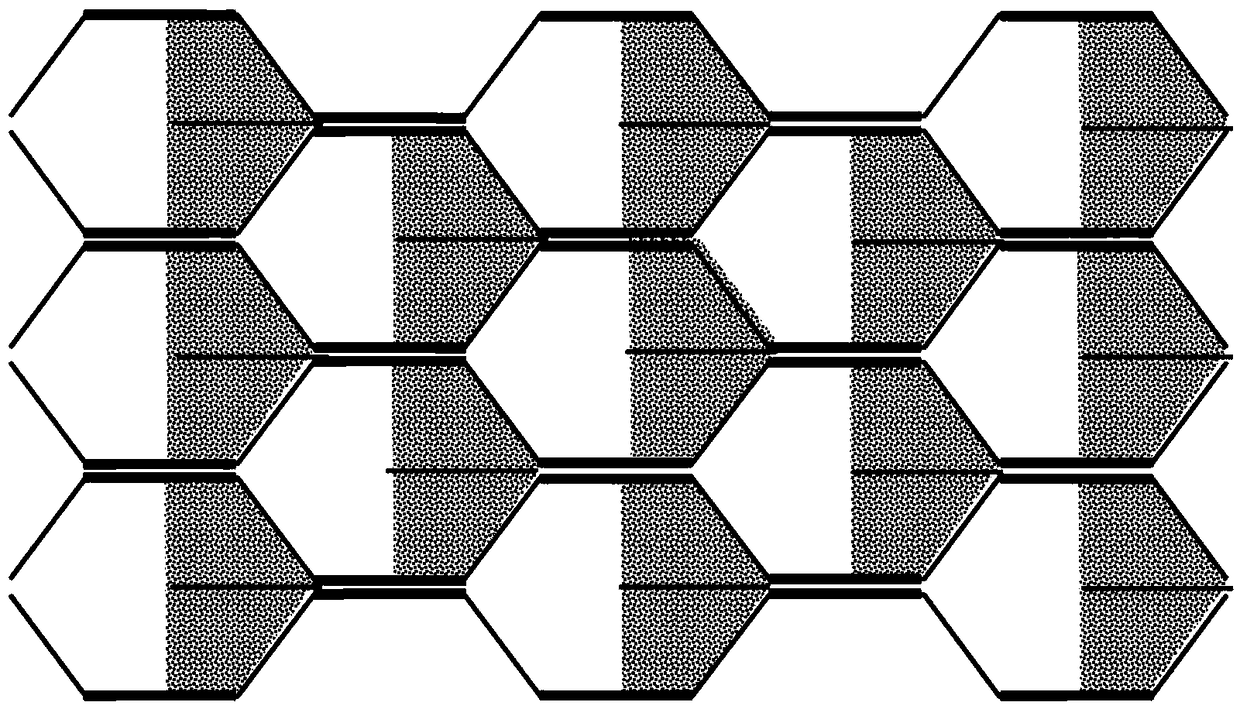
[0048] The surface density used in this embodiment is 80g / m 2 Nomex paper (Nomex paper) as substrate, need 25m 2 Flame Retardant Nomex Paper Production 1 m 2 The wave-absorbing honeycomb material weighs about 2.5kg and has a paper width of 0.9m. It produces a non-equilibrium hexagonal honeycomb with a side length of 0.55cm (the width of the node glue), using phenolic resin node glue, and the shape of the node glue is as follows: figure 2 As shown, the inclination angle is 45°. Superimposed and pressurized to form a 0.9m-high honeycomb substrate block and then sliced ​​into 14cm-high slices, and then cut one side of the honeycomb into 7cm-deep wedges with an electric saw. Then stretch and fix the honeycomb structure on the bracket to be 2.5m long, 1.2m wide and 0.14m high.

[0049] Graphene conductive coating formula: graphene (900ºC expands 450 times graphite ...

Embodiment 2

[0052] Example 2: Long-term use of wave-absorbing honeycomb with a height of 600 mm and a temperature of 120 °C

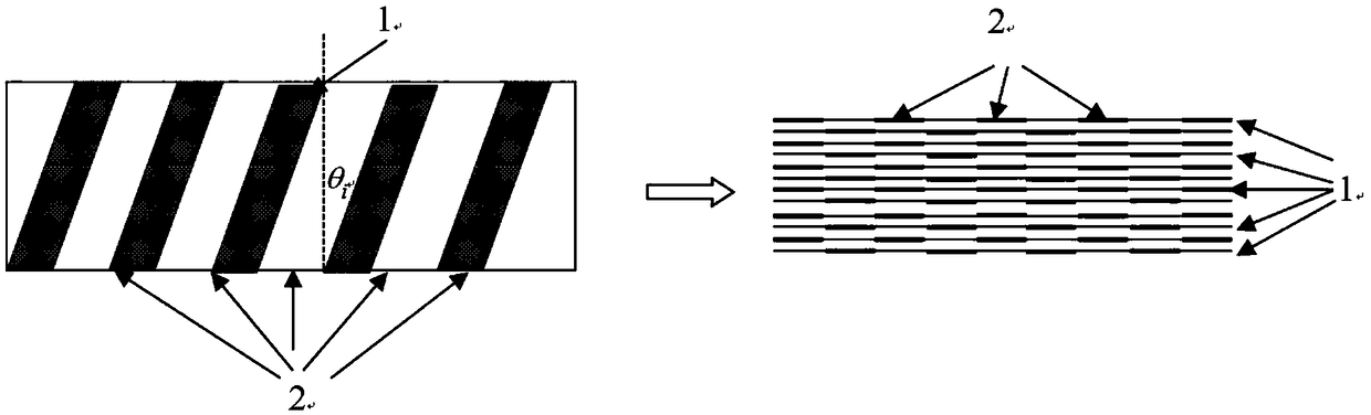
[0053] The surface density used in this embodiment is 180g / m 2 Kraft paper as the base material requires 38 m 2 Flame Retardant Kraft Paper Production 1 m 2 The absorbing honeycomb material weighs about 7.2kg and the paper width is 1.3m. First screen printed on paper as Figure 11 The conductive pattern of the inclined cone shown has a height of 0.6m, a width of the cone of 4.5cm, and an inclination angle of  i =30°, the length of the cone is half of the height, and then cured at 180°C for 30 minutes. Produce non-equilateral hexagonal honeycombs with a side length of 1.5cm (the width of the joint glue) and 3cm (the distance between the joint glue), use phenolic joint glue, and use the silk screen to print the joint glue continuously. The shape of the joint glue is as follows: Figure 7 ), the inclination angle of node glue printing is 30º, the height of each ...

Embodiment 3

[0057] Example 3: 1200mm high 120°C low-frequency wave-absorbing honeycomb

[0058] This embodiment uses surface density 180g / m 2 Kraft paper as the base material requires 48 m 2 Kraft paper production 1 m 2 The wave-absorbing honeycomb material weighs about 8.7kg and has a paper width of 1.3m. It produces non-equilateral hexagonal honeycombs with a side length of 2.5cm (the width of the joint glue) and 5cm (the distance between the joint glue) and an inclination angle of 30°. Use phenolic joint glue, the shape of the joint glue is as Figure 7 ), the height of each section is 32cm, the distance between the two sections of joint glue is 12cm, the horizontal displacement of the upper and middle joint glue is 3.75cm, the upper and lower joint glue are aligned, and the sheets are cut into 1.2m high honeycomb substrate blocks after being superimposed and pressurized and cured, and then The honeycomb structure stretched and fixed on the support is 2.5m long, 1.2m wide and 1.2m ...


PUM

PropertyMeasurementUnit
viscosityaaaaaaaaaa
particle sizeaaaaaaaaaa
specific surface areaaaaaaaaaaa

Abstract

The invention belongs to the technical field of microwave absorbing materials. The invention discloses a kind of super-wide incidence angle microwave absorbing materials which are composed of a slanted irregular honeycomb structure made of a flexible substrate and a graphene conductive coating coated on the flexible substrate. The invention also discloses a production method of the super-wide incidence angle microwave absorbing materials. The method comprises the steps of the structural design of the super-wide incidence angle microwave absorbing materials, generation of surface resistance distribution through printing the graphene conductive coating on the flexible materials, manufacturing of the slanted irregular honeycomb structure, etc. The super-wide incidence angle microwave absorbing materials have the microwave absorbing frequencies ranging from millimeter wave to microwaves and incidence angles ranging from normal incidence angles to high incidence angles. Meanwhile, the material has the advantages such as low cost, a high technique, being environment-friendly, high mechanical strength, low density, a long service life, high temperature resistance and flame retardancy. Furthermore, the super-wide incidence angle microwave absorbing materials of the invention can be contracted to keep, can reduce cost for transport and collection and is in favor of construction and usage of secret test external fields.

Description

technical field [0001] The invention relates to the technical field of microwave absorbing materials, in particular to an ultra-wide incident angle microwave absorbing material and a preparation method thereof. Background technique [0002] The existing absorbing anechoic chamber materials are basically designed and optimized according to the requirements of normal incidence. The design of the anechoic chamber is also affected by the performance of the material, and ample free space is basically used to reduce the influence of the reflective wall. If the space requirement of the anechoic chamber is reduced, the cost of the anechoic chamber can be reduced, but more electromagnetic waves and absorbing materials form high incident angle absorption. When designing an anechoic chamber, according to the application requirements, the incident angle range of each part is basically unchanged, and most anechoic chambers belong to this type of anechoic chamber. At this time, it is not ...

Claims


Application Information

Patent Timeline
Patent Type & Authority Applications(China)
IPC IPC(8): H05K9/00C09D161/14C09D5/24
CPCH05K9/0081C09D5/24C09D161/14C08K3/042C08K3/04
Inventor 张旭寇亚虎邓超然
Owner 西安安聚德纳米科技有限公司
Why Eureka
Try Eureka