A current protection chip and a manufacturing method thereof

A technology of current protection and manufacturing method, applied in circuits, electrical components, electrical solid devices, etc., can solve the problems of increasing device area and manufacturing cost, etc.

Active Publication Date: 2018-12-11
佛山市劲电科技有限公司
View PDF8 Cites 1 Cited by
  • Summary
  • Abstract
  • Description
  • Claims
  • Application Information

AI Technical Summary

Problems solved by technology

[0004] Currently commonly used current protection chips, if bidirectional protection is required, multiple current protection chips need to be connected in series or in parallel, which increases the device area and manufacturing cost

Method used


Image

  • A current protection chip and a manufacturing method thereof
  • A current protection chip and a manufacturing method thereof
  • A current protection chip and a manufacturing method thereof

Examples


Embodiment Construction

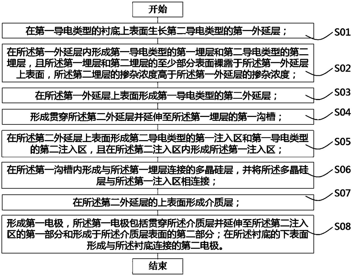
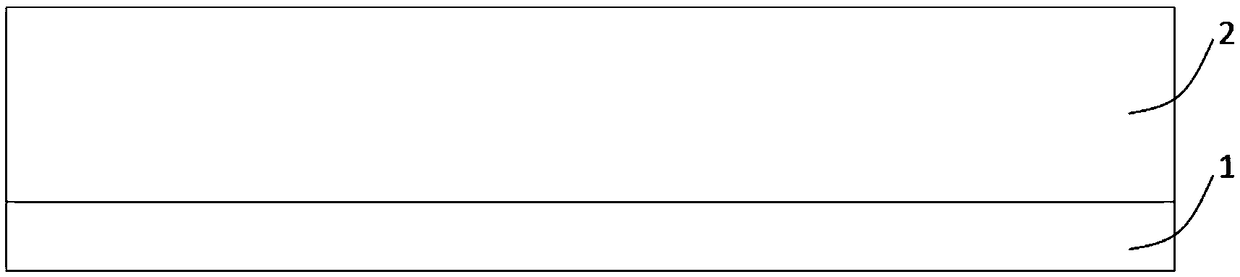
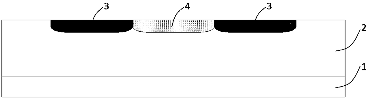
[0040] The invention will be described in more detail below with reference to the accompanying drawings. In the various figures, the same elements are indicated with similar reference numerals. For the sake of clarity, various parts in the drawings have not been drawn to scale. Also, some well-known parts may not be shown. For the sake of simplicity, the semiconductor structure obtained after several steps can be described in one figure.

[0041] It should be understood that when describing the structure of a device, when a layer or a region is referred to as being "on" or "over" another layer or another region, it may mean being directly on another layer or another region, or Other layers or regions are also included between it and another layer or another region. And, if the device is turned over, the layer, one region, will be "below" or "beneath" the other layer, another region.

[0042] If the purpose is to describe the situation directly on another layer or another a...


PUM


Abstract

The invention provides a current protection chip and a manufacturing method thereof. The current protection chip comprises a substrate of a first conductivity type; afirst epitaxial layer of a secondconductivity type; afirst buried layer of a first conductivity type and a second buried layer of a second conductivity type, formed in the first epitaxial layer; asecond epitaxial layer of a first conductivity type formed on a surface of the first epitaxial layer; afirst injection region of a second conductivity type and a second injection region of the first conductivity type, formed on a surfaceof the second epitaxial layer, and the second injection region is located in the first injection region; apolycrystalline silicon layer connected to the first implantation region and the first buriedlayer, respectively; adielectric layer formed on an upper surface of the second epitaxial layer; afirst electrode including a first portion penetrating the dielectric layer and extending to the second implantation region and a second portion formed on a surface of the dielectric layer; asecond electrode formed on a lower surface of the substrate and connected to the substrate. The invention can improve device performance and reduce device cost.

Description

technical field [0001] The invention relates to the technical field of semiconductors, in particular to a current protection chip and a manufacturing method thereof. Background technique [0002] The current protection chip is a solid-state semiconductor device specially designed to protect sensitive semiconductor devices from transient voltage surge damage. It has small clamping coefficient, small size, fast response, small leakage current and reliability. High advantages, so it has been widely used in voltage transient and surge protection. The low-capacitance current protection chip is suitable for high-frequency circuit protection devices, because it can reduce the interference of parasitic capacitance on the circuit and reduce the attenuation of high-frequency circuit signals. [0003] Electrostatic discharge, as well as other random voltage transients in the form of voltage surges, are commonly found in a variety of electronic devices. As semiconductor devices are in...

Claims


Application Information

Patent Timeline
Patent Type & Authority Applications(China)
IPC IPC(8): H01L27/02H01L27/08H01L29/861
CPCH01L27/0255H01L27/0814H01L29/861
Inventor 不公告发明人
Owner 佛山市劲电科技有限公司
Why Eureka
Try Eureka