How to make a photodetector

A technology of photodetectors and manufacturing methods, applied in the direction of circuits, electrical components, semiconductor devices, etc., can solve problems such as cost increase, low device yield, and complicated device manufacturing process, and achieve the effect of low loss and low optical transmission loss

Active Publication Date: 2020-04-07
INST OF SEMICONDUCTORS - CHINESE ACAD OF SCI
View PDF6 Cites 0 Cited by
  • Summary
  • Abstract
  • Description
  • Claims
  • Application Information

AI Technical Summary

Problems solved by technology

In Document 1, the detector material and the waveguide material without p-type doping are monolithically integrated using the butt coupling technology. Although a low transmission loss waveguide is obtained, the manufacturing process of the device is relatively complicated, involving corrosion and epitaxy processes that require precise control. Lead to low device yield and increased cost

Method used


Image

  • How to make a photodetector
  • How to make a photodetector
  • How to make a photodetector

Examples


Embodiment Construction

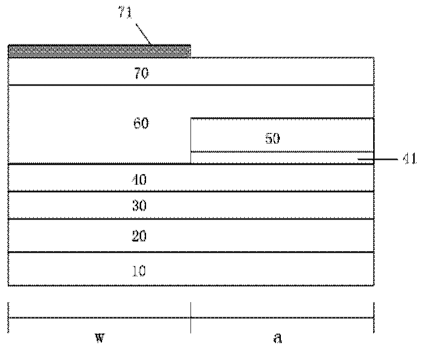
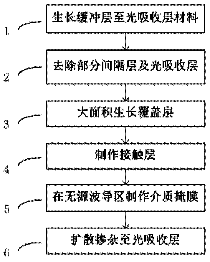
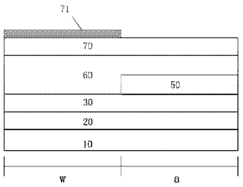
[0026] Please refer to the first example of figure 1 and figure 2 As shown, taking the InP-based material system as an example, the present invention provides a method for manufacturing a photodetector, which includes the following steps:

[0027] Step 1: growing an InP buffer layer 20 , an InGaAsP waveguide layer 30 , an InP light collecting layer 40 , an InGaAsP spacer layer 41 , and an InGaAs light absorbing layer material 50 sequentially on the InP substrate 10 . Wherein the InGaAsP waveguide layer 30 is doped with Si as the n-type contact material of the detector, the InP light collection layer 40 is not doped or low-concentration doped, and the InGaAs light absorption layer material 50 is not doped. The InGaAsP spacer material 41 can reduce the influence of the conduction bandgap difference between the InP light collecting layer 40 and the InGaAs light absorbing layer 50, and is composed of one layer of InGaAsP with a single wavelength or two layers of InGaAsP with two...


PUM


Abstract

The invention relates to a manufacturing method of a photodetector. The method includes the following steps: (1) sequentially growing a buffer layer, a waveguide layer, a light collecting layer, a spacer layer and a light absorbing layer on a substrate; 2, selectively removinga part of that spacer layer and the light absorption layer, wherein the removed part is a passive waveguide region and thereserved part is an absorption region; 3, grow a covering layer on that light collect layer and the light absorbing layer in a large area; 4, for a contact layer on that cover layer; 5, fabricate a dielectric mask on that contact layer in the passive waveguide region; 6, dope that light absorption layer, the clad layer and the contact layer above the absorption region in a diffusion doping mode. The invention can simplify the monolithic integration of the photodetector and the low-loss passive waveguide.

Description

technical field [0001] The invention relates to the field of optoelectronic devices, in particular to a method for manufacturing a photodetector. Background technique [0002] Photodetectors convert optical signals into electrical signals and are central components of systems such as fiber optic communications. In the single-row carrier detector, the absorption region is doped with p-type, and only photogenerated electrons are transported in the device. Due to the small effective mass of electrons, their transport speed is higher than that of holes, so the single-line carrier detection region has the advantages of high bandwidth, high saturated output power and low operating voltage, and has attracted extensive attention in recent years. Compared with multiple discrete devices, in order to achieve the same function, optoelectronic integrated chips have the advantages of small size and low power consumption, which can greatly improve the performance of optical fiber communic...

Claims


Application Information

Patent Timeline
Patent Type & Authority Patents(China)
IPC IPC(8): H01L31/18H01L31/109H01L31/0232
CPCH01L31/02327H01L31/109H01L31/1844Y02P70/50
Inventor 梁松刘云龙
Owner INST OF SEMICONDUCTORS - CHINESE ACAD OF SCI
Why Eureka
Try Eureka