Monolithic integrated surface emitting semiconductor laser based on supersurface and preparation method thereof

A metasurface and laser technology, applied in the structure of optical resonators and other directions, can solve the problems of complex preparation process, single output beam shape, large lasing threshold, etc., and achieve the effect of simple processing technology, compact structure and simplified preparation process.

Active Publication Date: 2018-12-11
HUAZHONG UNIV OF SCI & TECH
View PDF4 Cites 17 Cited by
  • Summary
  • Abstract
  • Description
  • Claims
  • Application Information

AI Technical Summary

Problems solved by technology

[0005] For the above defects or improvement needs of the prior art, the present invention provides a metasurface-based monolithic integrated surface-emitting semiconductor laser and its preparation method, thereby solving the problem of traditional surface-emitting semiconductor lasers (such as vertical cavity surface-emitting lasers) It is necessary to grow the upper and lower distributed Bragg reflector layers, and the preparation process is complex, the lasing threshold is large, and the technical problems of the output beam form are single

Method used


Image

  • Monolithic integrated surface emitting semiconductor laser based on supersurface and preparation method thereof
  • Monolithic integrated surface emitting semiconductor laser based on supersurface and preparation method thereof
  • Monolithic integrated surface emitting semiconductor laser based on supersurface and preparation method thereof

Examples


Embodiment Construction

[0028] In order to make the object, technical solution and advantages of the present invention clearer, the present invention will be further described in detail below in conjunction with the accompanying drawings and embodiments. It should be understood that the specific embodiments described here are only used to explain the present invention, not to limit the present invention. In addition, the technical features involved in the various embodiments of the present invention described below can be combined with each other as long as they do not constitute a conflict with each other.

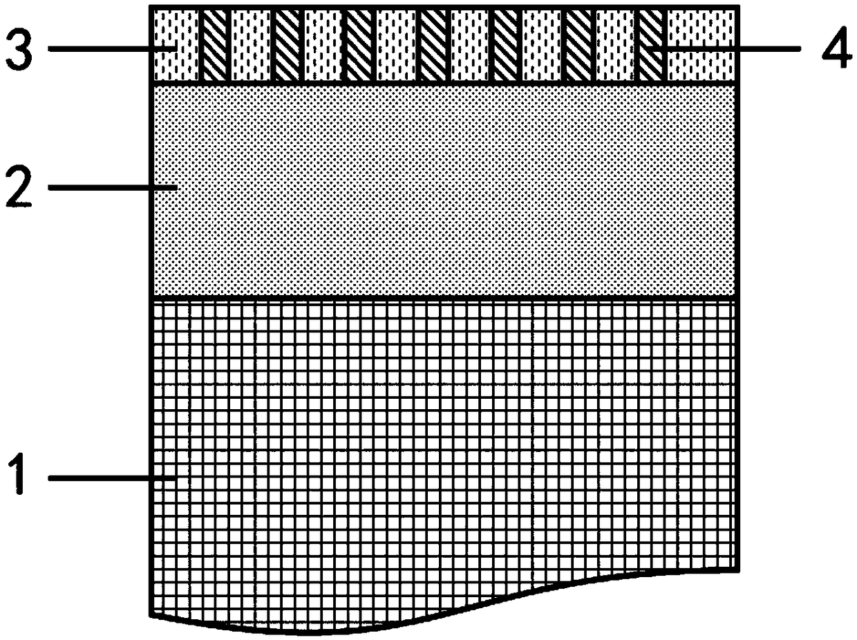
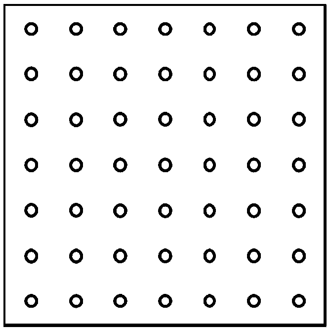
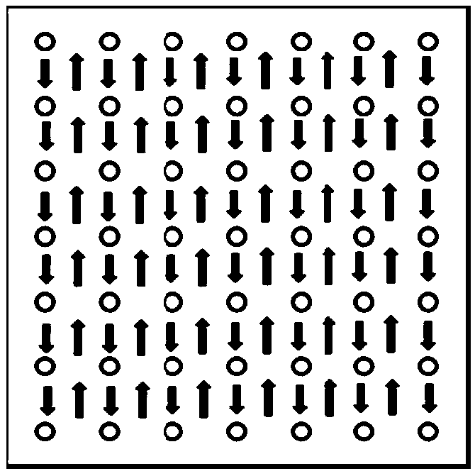
[0029] Aiming at the problem that the output beam of traditional semiconductor lasers has a single shape and needs a specific lasing threshold, the present invention proposes a metasurface structure made of the active layer structure of the semiconductor laser, and the resonant metasurface can be used to localize the light field in the Subwavelength scale and enhancement, planar subwavelength st...


PUM


Abstract

The invention discloses a monolithic integrated surface emitting semiconductor laser based on a super surface micro-nano structure. A super-surface micro-nano structure is combined with the active medium of semiconductor laser, the cluster coherent oscillation of the resonant unit inside the super-surface can be excited when the active material emits light in the active region. This local oscillation has high optical field binding ability and can provide positive feedback for the active layer to realize lasing. At the same time, by optimizing the structure of the super-surface micro-nano, we can control the far-field distribution characteristics of the beam, such as directional angle, phase, polarization, mode and so on. The laser structure comprises a substrate, a low refractive index layer, an active layer and a super-surface micro-nano structure. The preparation method comprises design and preparation of a light field confinement layer, a gain medium and the super-surface structure.Through the invention, the light field can be strongly localized in the near field, the far field distribution can be regulated by the arrangement mode of the structural unit, and the light field canbe directly regulated.

Description

technical field [0001] The invention belongs to the field of semiconductor lasers, and more specifically relates to a monolithic integrated vertical surface emitting semiconductor laser based on a metasurface microstructure and a preparation method thereof. Background technique [0002] Semiconductor lasers have a wide range of operating wavelengths, small size, mature processing and preparation technology, stable device performance, diverse applications, and low prices. They are widely used in optical communications, optical discs, laser printing, laser scanning and other fields, and have huge application requirements. Moreover, it can be pumped to emit light by means of electrical injection through a simple electrode structure, and the operating voltage and current of electrical injection are compatible with integrated circuits, and can be monolithically integrated with electrical devices and systems. Its modulation rate can reach GHz level, and it is widely used in optica...

Claims


Application Information

Patent Timeline
Patent Type & Authority Applications(China)
IPC IPC(8): H01S5/18H01S5/12
CPCH01S5/12H01S5/18
Inventor 夏金松崔成聪曾成袁帅
Owner HUAZHONG UNIV OF SCI & TECH
Why Eureka
Try Eureka