Cover plate and manufacturing method thereof, display panel and display device

A manufacturing method and cover plate technology, which is applied in semiconductor/solid-state device manufacturing, electrical components, diodes, etc., can solve the problems of complicated manufacturing process steps, large space occupied by the cover plate, and high production cost

Active Publication Date: 2018-12-14
BOE TECH GRP CO LTD
View PDF3 Cites 12 Cited by
  • Summary
  • Abstract
  • Description
  • Claims
  • Application Information

AI Technical Summary

Problems solved by technology

[0005] The present invention provides a cover plate and its manufacturing method, a display panel and a display device, so as to solve the problem that auxiliary cathodes and optic...

Method used


Image

  • Cover plate and manufacturing method thereof, display panel and display device
  • Cover plate and manufacturing method thereof, display panel and display device
  • Cover plate and manufacturing method thereof, display panel and display device

Examples


Embodiment 1

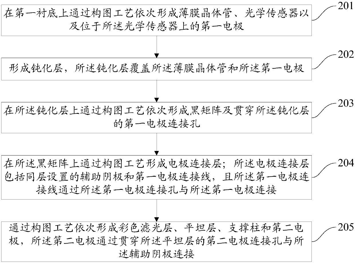
[0060] refer to figure 2 , which shows a flow chart of a method for manufacturing a cover plate according to an embodiment of the present invention, which may specifically include the following steps:

[0061] Step 201 , sequentially forming a thin film transistor, an optical sensor, and a first electrode on the optical sensor on a first substrate through a patterning process.

[0062] In the embodiment of the present invention, a thin film transistor is formed on the first substrate through a patterning process, an optical sensor is formed on the drain of the thin film transistor, and a first electrode is formed on the optical sensor.

[0063] Wherein, the drain of the thin film transistor is used as the lower electrode of the optical sensor at the same time, and the first electrode is the upper electrode of the optical sensor; the first electrode can be made of a transparent conductive material, such as ITO (Indium Tin Oxide, indium tin oxide) or IZO (Indium Zinc Oxide, in...

Embodiment 2

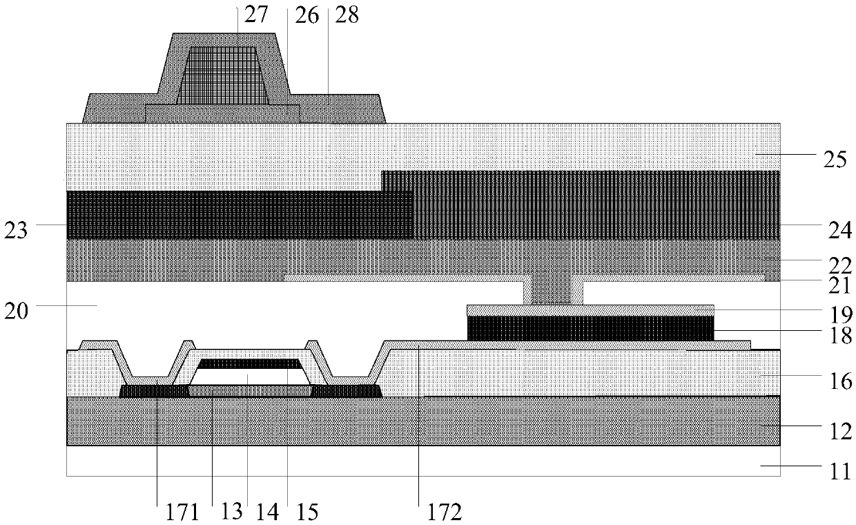
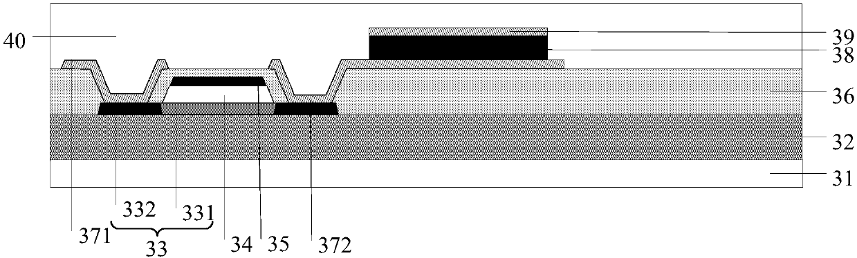
[0096] An embodiment of the present invention provides a cover plate, including a first substrate 31; a thin film transistor formed on the first substrate 31 in sequence, an optical sensor 38, and a first electrode 39 located on the optical sensor 38; a passivation layer 40 , the passivation layer 40 covers the thin film transistor and the first electrode 39; the black matrix 41 formed on the passivation layer 40; the electrode connection layer 42 formed on the black matrix 41, the electrode connection layer 42 includes an auxiliary cathode arranged on the same layer 421 and the first electrode connection line 422, and the first electrode connection line 422 is connected to the first electrode 39 through the first electrode connection hole M penetrating the passivation layer 40; the color filter layer 43, the flat layer 44, the support layer formed in sequence The pillar 45 and the second electrode 46 , the second electrode 46 is connected to the auxiliary cathode 421 through t...

Embodiment 3

[0103] An embodiment of the present invention provides a display panel, which includes the above-mentioned cover plate.

[0104] refer to Figure 10 , shows a schematic structural diagram of a display panel according to an embodiment of the present invention.

[0105] In the embodiment of the present invention, the display panel further includes a display substrate, the cover plate is fastened on the display substrate, and the display substrate includes: an anode 52, an organic light-emitting layer 53 and a cathode 54 stacked on the second substrate 51, and the cathode 54 In contact with the second electrode 46 .

[0106] Such as Figure 10 As shown, the contact position between the cathode 54 and the second electrode 46 is located at the position where the support column 45 is located.

[0107] Wherein, the material that cathode 54 adopts is a transparent conductive material, such as ITO or IZO etc.; The cathode 54 is contacted with the second electrode 43, and the second ...


PUM

PropertyMeasurementUnit
Thicknessaaaaaaaaaa
Thicknessaaaaaaaaaa
Thicknessaaaaaaaaaa

Abstract

The invention provides a cover plate and a manufacturing method thereof, a display panel and a display device, which relate to the technical field of display. A thin film transistor, an optical sensorand a first electrode located on the optical sensor are are sequentially formed on a first substrate by a composition process, a passivation layer is formed, a black matrix and a first electrode connection hole penetrating the passivation layer are sequentially formed on the passivation layer through a composition process, An electrode connecting layer is formed on the black matrix by a composition process, the electrode connecting layer comprising an auxiliary cathode and a first electrode connecting wire arranged in the same layer, and the first electrode connecting wire is connected with the first electrode through a first electrode connecting hole, and a color filter layer, a flat layer, a support column and a second electrode are sequentially formed by the composition process. As theauxiliary cathode and the first electrode connecting wire are formed by the one-time composition process, the manufacturing process steps are reduced, the manufacturing cost is reduced, and the auxiliary cathode and the first electrode connecting wire are arranged on the same layer, so that the occupied space of the cover plate can be saved.

Description

technical field [0001] The invention relates to the field of display technology, in particular to a cover plate and a manufacturing method thereof, a display panel and a display device. Background technique [0002] The OLED (Organic Light-emitting Diode, Organic Light-Emitting Diode) display panel may include a top-emitting OLED display panel and a bottom-emitting OLED display panel. The light of the top-emitting OLED display panel is emitted from the cathode side. Therefore, in order to ensure the To increase the transmittance, the thickness of the cathode needs to be reduced, but as the thickness of the cathode decreases, the resistance of the cathode increases. Therefore, an auxiliary cathode can be made on the cover plate in the top emission OLED display panel to reduce the resistance of the cathode, thereby improving the top. The display quality of the emissive OLED display panel; at the same time, in order to further improve the display quality of the OLED display pan...

Claims


Application Information

Patent Timeline
IPC IPC(8): H01L27/32H01L51/52
CPCH10K59/88H10K59/00H10K59/123H10K59/12H10K50/84H10K59/13H10K50/824H10K50/841H10K50/828H10K50/865H10K59/38H10K59/60H10K71/00
Inventor 李伟刘威
Owner BOE TECH GRP CO LTD
Why Eureka
Try Eureka