
Evaporation system, and preparation method for OLED device

A light-emitting device and evaporation technology, which is applied in the manufacture of semiconductor/solid-state devices, electric solid-state devices, semiconductor devices, etc., can solve the problems of uneven color of OLED light-emitting devices, weakening of the strength of fine metal masks, and prone to wrinkles. Achieve the effect of reducing the risk of wrinkling, reducing density and reducing the risk of manufacturing

Inactive Publication Date: 2018-12-18
WUHAN CHINA STAR OPTOELECTRONICS SEMICON DISPLAY TECH CO LTD
View PDF5 Cites 5 Cited by
  • Summary
  • Abstract
  • Description
  • Claims
  • Application Information

AI Technical Summary

Problems solved by technology

[0005] The embodiment of the present application provides an evaporation system and a method for preparing an OLED light-emitting device; in order to solve the problem that the existing method for preparing an OLED light-emitting device has a large number of openings in the fine metal mask, which causes the strength of the fine metal mask to weaken and is prone to occur Wrinkles, which in turn lead to technical problems such as color unevenness and poor appearance of OLED light-emitting devices

Method used


Image

  • Evaporation system, and preparation method for OLED device
  • Evaporation system, and preparation method for OLED device
  • Evaporation system, and preparation method for OLED device

Examples


Embodiment Construction

[0052] Please refer to the drawings in the accompanying drawings, wherein like reference numerals refer to like components. The following description is based on illustrated specific embodiments of the present application, which should not be construed as limiting other specific embodiments of the present application that are not described in detail here.

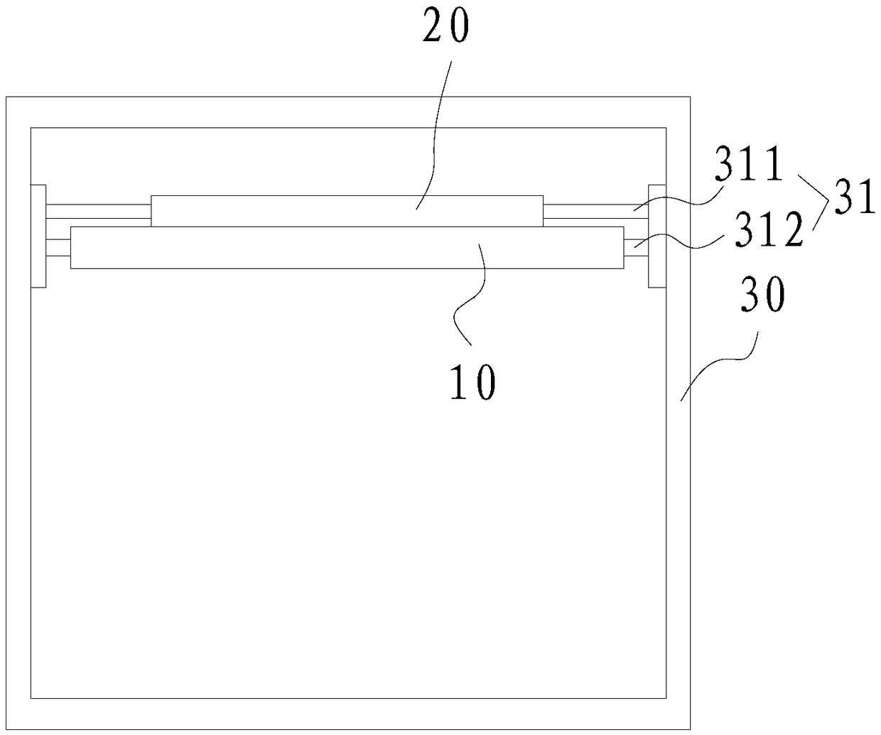
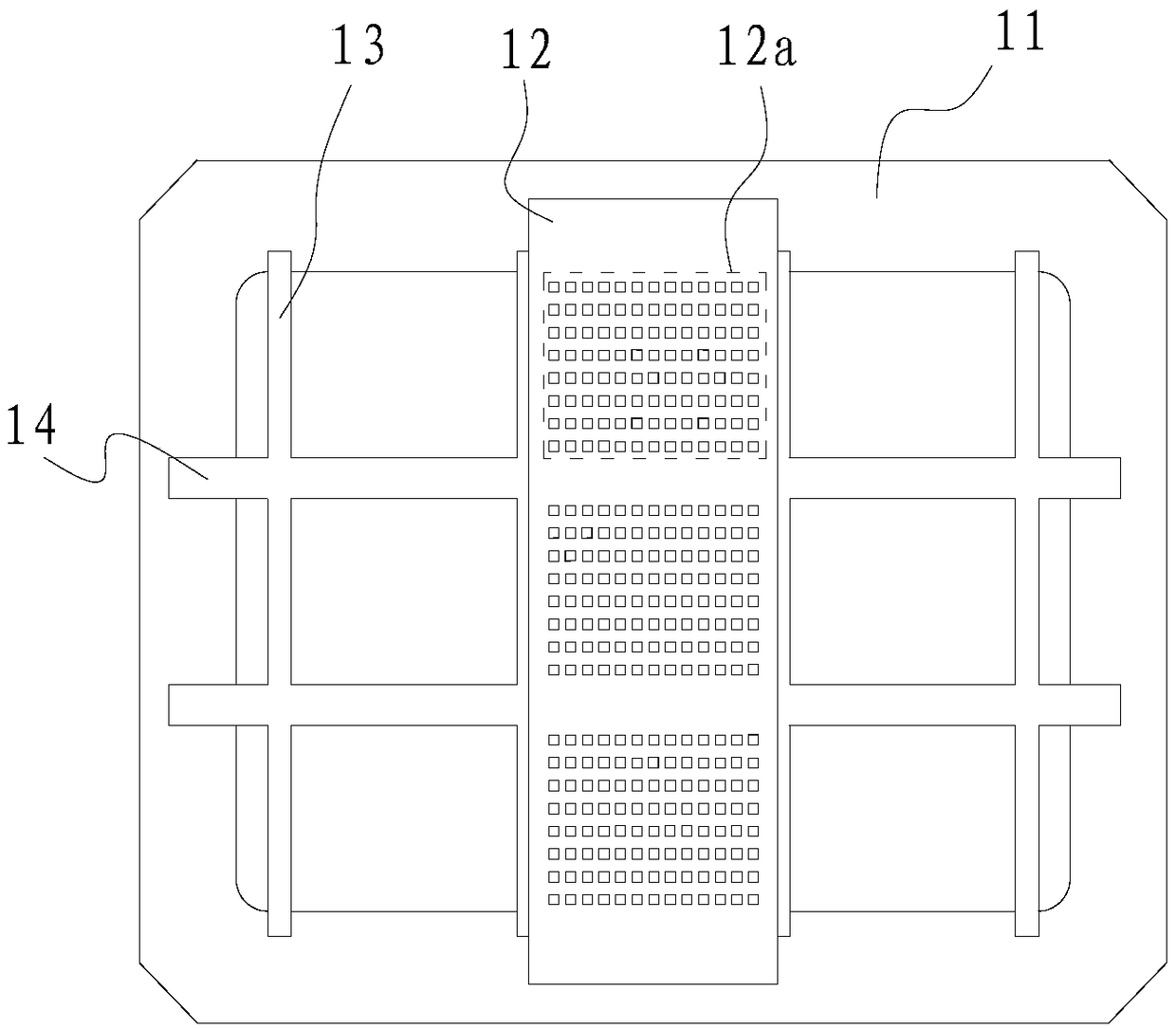
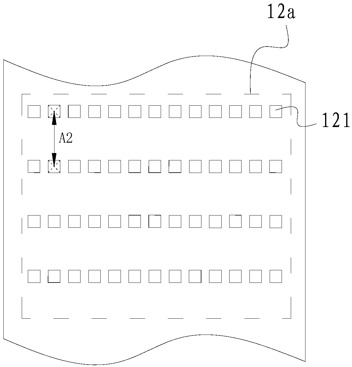
[0053] Please refer to Figure 1 to Figure 4 , figure 1 It is a schematic structural diagram of the first embodiment of the evaporation system of the present application; figure 2 It is a schematic structural diagram of the mask assembly of the first embodiment of the evaporation system of the present application; image 3 It is a schematic structural diagram of the evaporation area of ​​the mask plate in the first embodiment of the evaporation system of the present application; Figure 4 It is a schematic structural diagram of the sub-pixel image corresponding to the mask plate in the first embodiment of the evaporatio...


PUM


Abstract

The application provides an evaporation system, and a preparation method for an OLED device. The evaporation system comprises a mask plate, and the mask plate comprises at least one evaporation area corresponding to an OLED baseplate, and evaporation holes formed in the evaporation area and used for forming sub-pixels of a sub-pixel pattern; the evaporation holes are arranged in a matrix, and thenumber of the sub-pixels is N times the number of the evaporation holes (N is an integer but no less than 2); and the evaporation holes are used for preparing a complete sub-pixel pattern through cooperation with offset of an evaporation machine. According to the evaporation system, through decrease of the number of the evaporation holes in the mask plate, the strength of the mask plate is improved, and the risk that wrinkles are generated during net laying is reduced; meanwhile, the phenomenon that the color of the OLED device is uneven during evaporation is avoided in the preparation methodfor the OLED device; and in addition, by adopting the OLED baseplate or the mask plate offset mode, the overall evaporation accuracy of the light-emitting sub-pixels is improved.

Description

technical field [0001] The present application relates to a display technology, in particular to an evaporation system and a method for preparing an OLED light-emitting device. Background technique [0002] Organic Light-Emitting Diode (OLED) displays are more and more popular in the market due to their active light emission, large viewing angle, wide color gamut, high brightness, and fast response speed. At the same time, the resolution of OLED displays is getting higher and higher. However, the current production of high-resolution, high-resolution OLED displays still faces many technical difficulties to be overcome. [0003] At present, the most common method of manufacturing OLED light-emitting devices is to use vacuum evaporation. The organic light-emitting material is heated in a crucible, from a solid state to a gaseous state, and then deposited on the corresponding array substrate through the openings of a fine metal mask. The pixel definition layer PDL (Pixel Defi...

Claims


Application Information

Patent Timeline
IPC IPC(8): C23C14/04C23C14/24H01L51/56H01L51/00
CPCC23C14/042C23C14/24H10K71/16H10K71/00
Inventor 叶剑
Owner WUHAN CHINA STAR OPTOELECTRONICS SEMICON DISPLAY TECH CO LTD
Learn More