Printed circuit board (PCB) high current test method

A test method and high-current technology, applied in the direction of electronic circuit testing, automated test systems, measuring electricity, etc., can solve the problems of destructive verification, inner-layer circuit connection problems, and high levels, to avoid scrap loss, adjustment and improvement, short time effect

Active Publication Date: 2018-12-18
威太(苏州)智能科技有限公司
View PDF10 Cites 6 Cited by
  • Summary
  • Abstract
  • Description
  • Claims
  • Application Information

AI Technical Summary

Problems solved by technology

In such a high-temperature process, the thermal expansion of the PCB board may cause problems in the connection of the inner layer circuits. Such problems will affect the integrity of the signal transmission of the PCB circuit, and there may also be a potential risk of electronic product function failure.
Usually this kind of problem has a higher level in the risk of PCB boards, and the scope of influence is wider, which will lead to huge economic compensation losses for PCB board production factories.
[0006] At present, most PCB board simulati

Method used


Image

  • Printed circuit board (PCB) high current test method
  • Printed circuit board (PCB) high current test method
  • Printed circuit board (PCB) high current test method

Examples


Example Embodiment

[0036] Example 1

[0037] A PCB high current test method, specifically including the following steps:

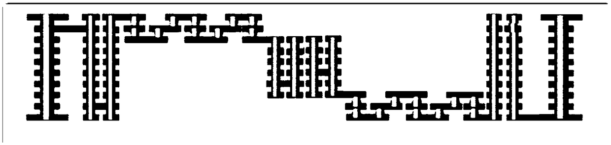
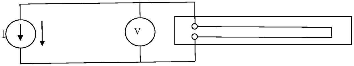
[0038] S1. Front resistance measurement: Use a four-wire micro-resistance meter to measure the resistance of both ends of the HCT Coupon test loop, (HCT Coupon wiring indication figure 1 (Shown), this link can detect PCB plating incompleteness problems. If the measured resistance value has a large deviation from the theoretical resistance value, the problem is mainly caused by the following possible factors such as: electroplating laser blind hole / through hole Hole breakage, laser blind hole missed / impermeable / small hole diameter, mechanical drilling missed drilling or drilling offset, compression combination group staggered type, etc.;

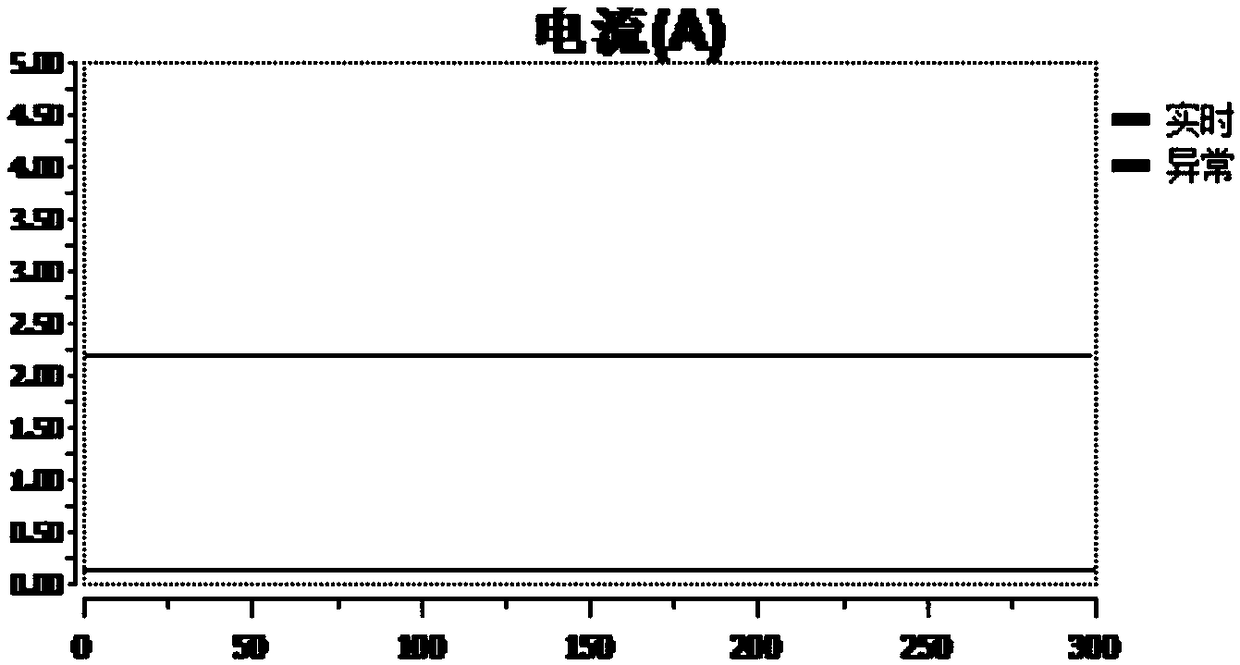
[0039] S2. If the front resistance test is passed, it will enter the high current test link (this link is to simulate high temperature production processes such as PCB overheated air reflow furnace or wave soldering, and the normal temperature in ...


PUM


Abstract

The invention discloses a printed circuit board (PCB) high current test method. The PCB high current test method comprises the steps of front resistance measurement, high current test, cooling, rear resistance measurement and resistance change rate calculation. Through the test of the five steps, the PCB high current test method can detect the problems in PCB products such as hole-bottom separation, non-penetrating lasers, laser no marking, blind-hole hole breakout, through-hole hole breakout, welding missing, laser breakdown, hole-bottom defective gum, foreign matter hole breakout, surface copper deficiency, through-hole ICD, bind-hole hole copper deficiency, small laser perforations, blind-hole folding plating, through-hole folding plating, copper powder inside holes, small laser holes and electroplating hole breakout; during the test, no damage is caused to the PCB products, the shipment of the products is not affected, and non-destructive test is achieved; and the consumed time oftest is relatively short, batch test can be carried out, the timeliness is good, the defect problems can be quickly fed back so as to timely adjust and improve the production process and avoid unnecessary scrap loss.

Description

Technical field [0001] The invention relates to the technical field of PCB testing, in particular to a PCB high-current testing method. Background technique [0002] PCB (PrintedCircuitBoard), the Chinese name is printed circuit board. As an important carrier of electronic components, PCB is combined with numerous electronic components to construct various electronic products that can be seen in life. Mobile phones, smart watches, computers, televisions, cars, satellites, space shuttles... [0003] With the advancement of science and technology, human living standards have been greatly improved, and people have put forward higher requirements for the safety and reliability of electronic products. Maybe the phone or computer occasionally black screen, you only need to reset or restart it, that will only affect your experience; if the battery of the phone catches fire and explodes, if the vehicle suddenly goes out of control at high speed, if the fighter missile suddenly fails. , ...

Claims


Application Information

Patent Timeline
IPC IPC(8): G01R31/28
CPCG01R31/2806G01R31/2834
Inventor 段景盛
Owner 威太(苏州)智能科技有限公司
Why Eureka
Try Eureka