Image sensor and method of forming the same

An image sensor and pixel area technology, applied in semiconductor devices, electrical solid state devices, radiation control devices, etc., can solve problems such as increased crosstalk and impact on image sensor performance.

Active Publication Date: 2021-01-22
淮安西德工业设计有限公司
View PDF3 Cites 0 Cited by
  • Summary
  • Abstract
  • Description
  • Claims
  • Application Information

AI Technical Summary

Problems solved by technology

[0004] However, with the improvement of device integration, the density of pixel units in image sensors increases, and the crosstalk between adjacent pixel units continues to increase, which affects the performance of image sensors.

Method used


Image

  • Image sensor and method of forming the same
  • Image sensor and method of forming the same
  • Image sensor and method of forming the same

Examples


Embodiment Construction

[0031] As mentioned in the background, prior art image sensors perform poorly.

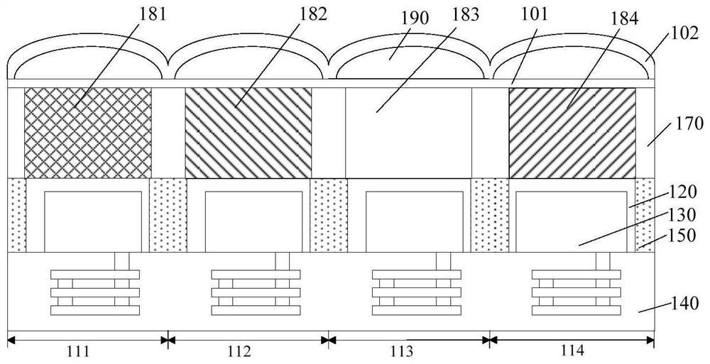
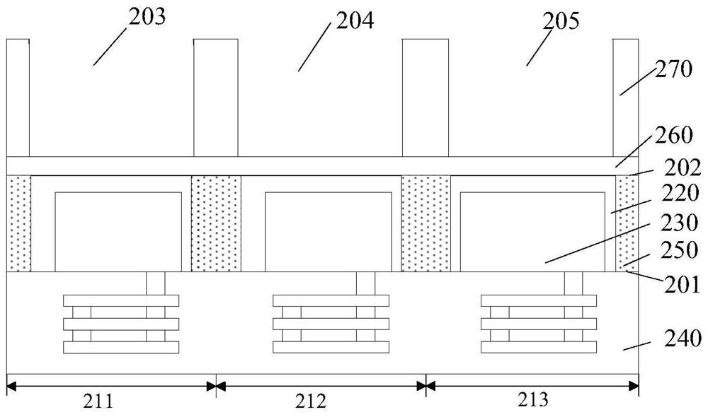
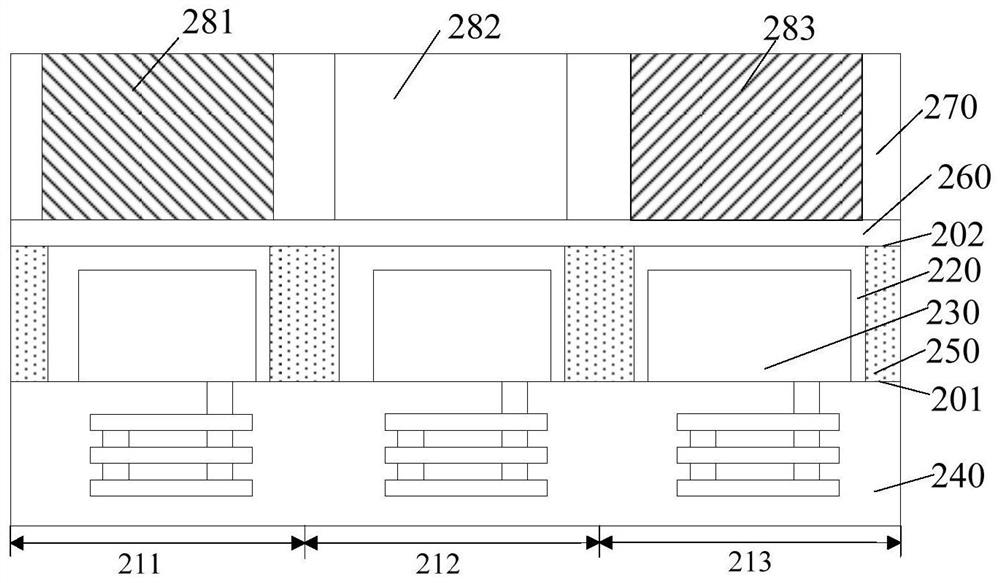
[0032] refer to figure 1 , figure 1It is a structural schematic diagram of an image sensor, the image sensor includes a plurality of pixel units, the pixel unit includes: a substrate 120, a photosensitive structure 130, an interconnection structure 140 and a light receiving structure, and the substrate 120 has an opposite first surface and a second surface, the photosensitive structure 130 is located in the substrate 120, the first surface of the substrate 120 exposes the photosensitive structure 130, and the interconnect structure 140 is in contact with the first surface of the substrate 120, so The light-receiving structure is located on the second surface of the substrate 120, the light-receiving structure includes a lens layer 190, a filter layer and a grid layer 170, the lens layer 190 is located on the surface of the filter layer, and the grid layer 170 is located between adjacent filter la...


PUM


Abstract

An image sensor and a forming method thereof are provided. The image sensor includes a substrate including a first pixel region and a second pixel region; a substrate surface in the first pixel regionprovided with a first filter lay for passing monochromatic light; a second filter layer for transmitting natural light on the surface of the substrate in the second pixel region; a first anti-reflective structure located in a first pixel region, the first anti-reflective structure comprising one or both of a first anti-reflective coating and a second anti-reflective coating, the first anti-reflective coating being located between the first filter layer and the substrate, the second anti-reflective coating being located on the first filter layer; a second anti-reflective structure located in the second pixel region, the second anti-reflective structure having a thickness smaller than the first anti-reflective structure, the second anti-reflective structure comprising one or both of a thirdanti-reflective coating and a fourth anti-reflective coating, the third anti-reflective coating being located between the second filter layer and the substrate, and the fourth anti-reflective coatingbeing located on the second filter layer. The performance of the image sensor is improved.

Description

technical field [0001] The invention relates to the field of semiconductor manufacturing, in particular to an image sensor and a forming method thereof. Background technique [0002] An image sensor is a semiconductor device that converts light signals into electrical signals. Image sensors are classified into complementary metal oxide (CMOS) image sensors and charge coupled device (CCD) image sensors. CMOS image sensor has the advantages of simple process, easy integration of other devices, small size, light weight, low power consumption and low cost. Therefore, with the development of image sensing technology, CMOS image sensors are increasingly used in various electronic products instead of CCD image sensors. At present, CMOS image sensors have been widely used in still digital cameras, digital video cameras, medical imaging devices, and automotive imaging devices. [0003] CMOS image sensors include front illuminated (FSI) image sensors and back illuminated (BSI) imag...

Claims


Application Information

Patent Timeline
Patent Type & Authority Patents(China)
IPC IPC(8): H01L27/146
CPCH01L27/1462H01L27/14621H01L27/1464H01L27/14645H01L27/14654H01L27/14683H01L27/14685
Inventor 何延强林宗德黄仁德李晓明
Owner 淮安西德工业设计有限公司
Why Eureka
Try Eureka