Method for fabricating flat free contact surfaces of semiconductor nanostructures

A nanostructure and semiconductor technology, which is applied in the field of vertically stacking multiple nanostructures and nanowires, can solve problems such as inability to realize applications, achieve effective controllability, and achieve the effect of vertical integration

Active Publication Date: 2022-03-25
FORSCHUNGSZENTRUM JULICH GMBH
View PDF22 Cites 0 Cited by
  • Summary
  • Abstract
  • Description
  • Claims
  • Application Information

AI Technical Summary

Problems solved by technology

This electrically short-circuits the nanowire along its growth axis and therefore does not enable the application in the sense of the present invention

Method used


Image

  • Method for fabricating flat free contact surfaces of semiconductor nanostructures
  • Method for fabricating flat free contact surfaces of semiconductor nanostructures
  • Method for fabricating flat free contact surfaces of semiconductor nanostructures

Examples


Embodiment Construction

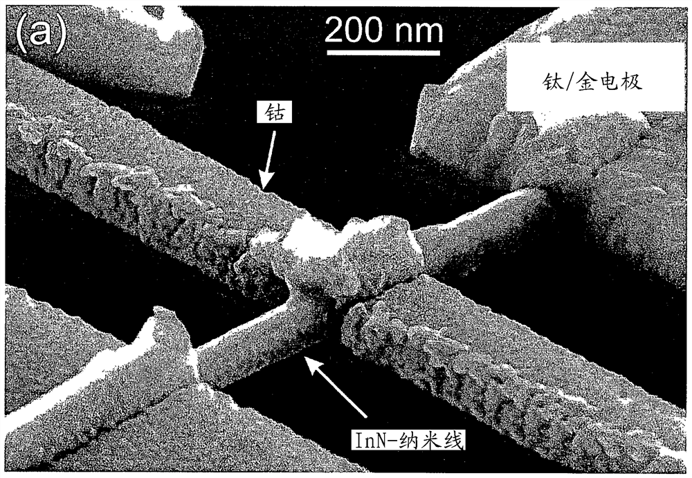
[0078] An unfavorable result that often occurs in conventionally evaporated nanowires with thin metal layers is identified in Fig. 1(a) with interruptions in the electrical contacts due to shadowing effects. In particular, ferromagnetic contacts, for example composed of cobalt, have a significant disturbance of the homogeneity of the magnetization, which is mandatory for several components of spintronics and is shown in Fig. 1(b) .

[0079] In Fig. 1(b), the calculated local magnetization is shown in cross-section along the cobalt contact surrounding this circular Nanowire cross-sections are laid. Here, the stated external magnetic field is applied along the main axis of the cobalt strip, ie perpendicular to the nanowire and parallel to the substrate.

[0080] Arrows inside cobalt contacts: local orientation of magnetic moments;

[0081] Highlighted in grey: localized magnetization points mostly to the right

[0082] Bright area: localized magnetization points mostly to th...


PUM

PropertyMeasurementUnit
lengthaaaaaaaaaa

Abstract

The invention relates to a method for producing planar free contact surfaces of semiconductor nanostructures, wherein at least one nanostructure (2) is arranged on the surface of a starting substrate (1) on the transfer substrate (1 ) is applied on the same surface of the first layer (3), said first layer embedding said at least one nanostructure (2), and a second substrate (5) is applied on said first layer (3) , wherein the transfer substrate (1) is subsequently separated from the first layer (3) such that at least one nanostructure (2) embedded therein has a planar free surface. According to the invention, an additional layer (6) dissolvable by a solvent is applied to the surface of the transfer substrate (1) before the at least one nanostructure (2) is applied to the transfer substrate (1) and the transfer substrate (1) is separated from the first layer (3) by means of a solvent. In this way planarization / stacking of the nanostructures and subsequent easy electrical contacting can be achieved. In the case of an iterative application of the method steps, multiple layers, for example consisting of horizontally oriented nanowire networks, can advantageously be built up ( FIG. 5B ).

Description

technical field [0001] The present invention relates to novel methods for planarizing nanostructures, in particular nanowires, eg prior to electrical contacting. The invention also relates to a method for vertically stacking a plurality of nanostructures, that is to say, for fabricating one or more layers with embedded nanowires or networks of nanowires or other nanostructures that can be electrically contacted. Background technique [0002] Self-organizing nanostructures, especially semiconductor nanowires, which have been the subject of intensive research for many years, could soon be used as basic building blocks in computer chips. This aspect is attributed to the significantly superior electron mobility in III / V semiconductor nanowires relative to conventional silicon CMOS technology. There are also possibilities for optoelectronic functions and the use of new types of electrically controllable magnetic functions in the field of spintronics and the use of nanowires in t...

Claims


Application Information

Patent Timeline
Patent Type & Authority Patents(China)
IPC IPC(8): H01L29/66H01L29/06H01L29/40H01L29/775B82Y10/00B82Y40/00
CPCB82Y10/00B82Y40/00H01L29/401H01L29/66469H01L29/775H01L29/0673
Inventor S.黑特J.格哈茨T.舍珀斯D.格吕茨马歇尔
Owner FORSCHUNGSZENTRUM JULICH GMBH
Why Eureka
Try Eureka