Beryllium mirror surface layer based on amorphous alloy and preparation method thereof

A technology of amorphous alloy and mirror layer, which is applied in the field of material science and engineering, can solve the problems of high cost and long process flow, and achieve the effects of low production cost, shortened process flow and strong controllability

Active Publication Date: 2019-01-04
MATERIAL INST OF CHINA ACADEMY OF ENG PHYSICS
View PDF7 Cites 3 Cited by
  • Summary
  • Abstract
  • Description
  • Claims
  • Application Information

AI Technical Summary

Problems solved by technology

[0004] The technical problem to be solved by the present invention is to provide a method for preparing a beryllium mirror surface layer based on an amorphous alloy, so as to solve the problems of long technological process and high cost in the processing of a beryllium mirror surface in the prior art

Method used


Image

  • Beryllium mirror surface layer based on amorphous alloy and preparation method thereof
  • Beryllium mirror surface layer based on amorphous alloy and preparation method thereof
  • Beryllium mirror surface layer based on amorphous alloy and preparation method thereof

Examples


Embodiment 1

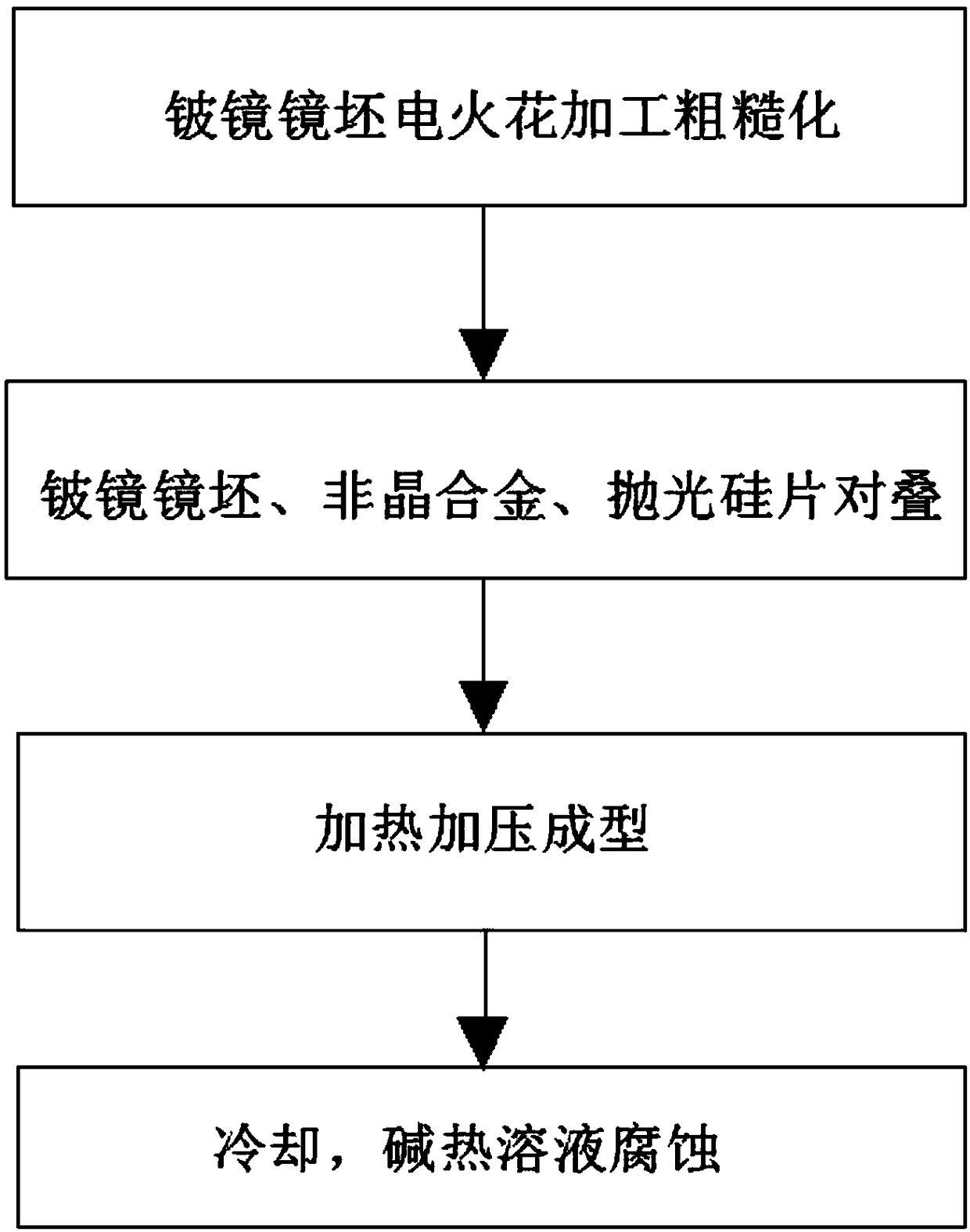
[0031] Preparation of small-sized beryllium mirror mirror layer based on amorphous alloy, the specific process is as follows figure 1 shown, including the following steps:

[0032] Step 1: Surface roughening of beryllium mirror blank:

[0033] Select a beryllium mirror blank with a diameter of about 10mm, and use electric discharge machining to process the beryllium surface of the beryllium mirror to roughen the surface and produce microscopic holes with a diameter of about 0.5mm and a depth of about 1mm.

[0034] Step 2: Beryllium mirror surface layer preparation of amorphous alloy:

[0035] choose Ni 62 PD 19 Si 2 P 17 The amorphous alloy thin slice and the polished silicon wafer both have a diameter of 10 mm and a thickness of the amorphous thin slice of 1 mm. The polished silicon wafer, the amorphous alloy thin slice and the beryllium mirror blank after the surface treatment in step 1 are stacked in sequence, wherein the polished surface of the polished silicon wafer...

Embodiment 2

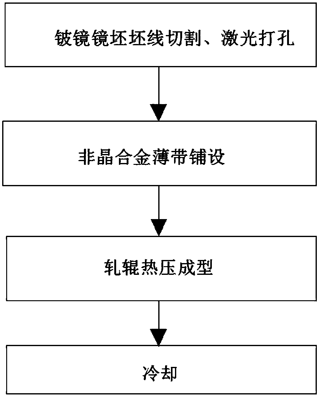
[0038] Preparation of mirror layer of large-sized beryllium mirror based on amorphous alloy, and its specific process flow figure 2 shown, including the following steps:

[0039] Step 1: Surface roughening of beryllium mirror blank:

[0040] Select a beryllium mirror blank with a diameter of about 50mm, and use wire cutting and laser drilling to process the beryllium surface of the beryllium mirror to make the surface rough. Among them, wire cutting produces micron-scale irregular fluctuations, which are randomly distributed on the entire surface of the beryllium mirror blank. Laser drilling produces micron empty arrays. The diameter of the holes is about 0.1mm, the depth is about 0.15mm, and the spacing is about 0.2mm.

[0041] Step 2: Beryllium mirror surface layer preparation of amorphous alloy:

[0042] Choose Zr 41.2 Ti 13.8 Cu 12.5 Ni 10 be 22.5 A thin strip of amorphous alloy with a thickness of about 35 μm. Spread the amorphous alloy thin strip on the surface-...


PUM

PropertyMeasurementUnit
thicknessaaaaaaaaaa
thicknessaaaaaaaaaa

Abstract

The invention discloses a beryllium mirror surface layer based on amorphous alloy and a preparation method thereof. The problems that in the prior, during beryllium mirror surface processing, the technology processes are long, and the cost is high are solved. According to the preparation method of the beryllium mirror surface layer based on amorphous alloy, under the pressure condition, the amorphous alloy is heated to a supercooling liquid phase temperature region, the amorphous alloy is subjected to thermoplastic forming, micro holes in beryllium mirror blanks are filled with the amorphous alloy, and then the beryllium mirror surface layer based on the amorphous alloy is obtained. The invention further discloses the beryllium mirror surface layer prepared by adopting the method. The beryllium mirror surface layer is scientific in design, simple in technology, high in controllability, low in production cost and environmentally friendly.

Description

technical field [0001] The invention belongs to the field of material science and engineering, and in particular relates to an amorphous alloy-based beryllium mirror surface layer and a preparation method thereof. Background technique [0002] Beryllium mirrors have irreplaceable applications in weapon aiming, space telescopes, weather satellites and other fields. However, beryllium mirror blanks are difficult to process, and there is a lot of beryllium oxide, so it is difficult to directly process to obtain a mirror surface. At present, Ni-P is often plated after single-point diamond processing, and then further mirror processing is performed. This method has a long technical process and high cost. [0003] Therefore, it is an urgent problem to be solved by those skilled in the art to provide a processing method of a beryllium mirror, which is simple, low in production cost, and has excellent space environment serviceability and corrosion resistance. Contents of the inv...

Claims


Application Information

Patent Timeline
Patent Type & Authority Applications(China)
IPC IPC(8): C23C26/00C22C45/10
CPCC22C45/10C23C26/00
Inventor 刘学李晋锋乐国敏曲凤盛王斗
Owner MATERIAL INST OF CHINA ACADEMY OF ENG PHYSICS
Why Eureka
Try Eureka