Heat dissipation substrate and preparation method thereof

A heat dissipation substrate and insulating base material technology, which is applied in the manufacture of semiconductor/solid-state devices, electrical components, electric solid-state devices, etc., can solve the problem of difficult heat diffusion in thick copper line areas, large wiring area of ​​heat dissipation substrates, unfavorable miniaturization of heat dissipation substrates, etc. problems, to achieve the effects of miniaturization, low cost, and improved withstand voltage performance

Active Publication Date: 2019-01-04
RAYBEN TECH ZHUHAI
View PDF8 Cites 4 Cited by
  • Summary
  • Abstract
  • Description
  • Claims
  • Application Information

AI Technical Summary

Problems solved by technology

[0005] In the above prior art, on the one hand, both the thick copper circuit area and the thin copper circuit area are arranged on the surface of the heat dissipation substrate, resulting in a larger wiring area required by the heat dissipation substrate, which is not conducive to the miniaturization of the heat dissipation substrate; on the other hand, the ceramic The heat sink passes through the thick copper line area, and the heat in the thick copper line area is difficult to spread quickly through the ceramic heat sink
In addition, the above-mentioned preparation method of the heat dissipation substrate needs to provide the first core board and the second core board, the preparation process is complicated and the cost is high

Method used


Image

  • Heat dissipation substrate and preparation method thereof
  • Heat dissipation substrate and preparation method thereof
  • Heat dissipation substrate and preparation method thereof

Examples


Embodiment 1

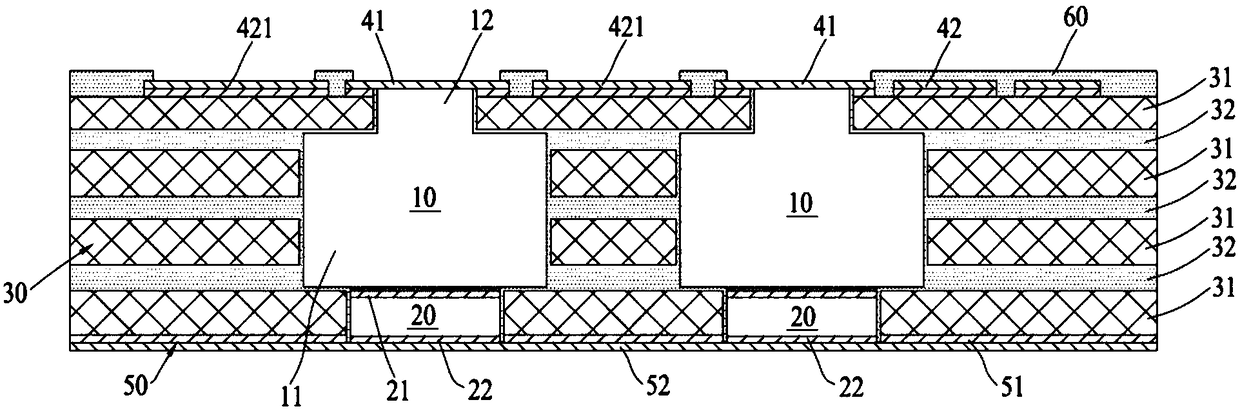
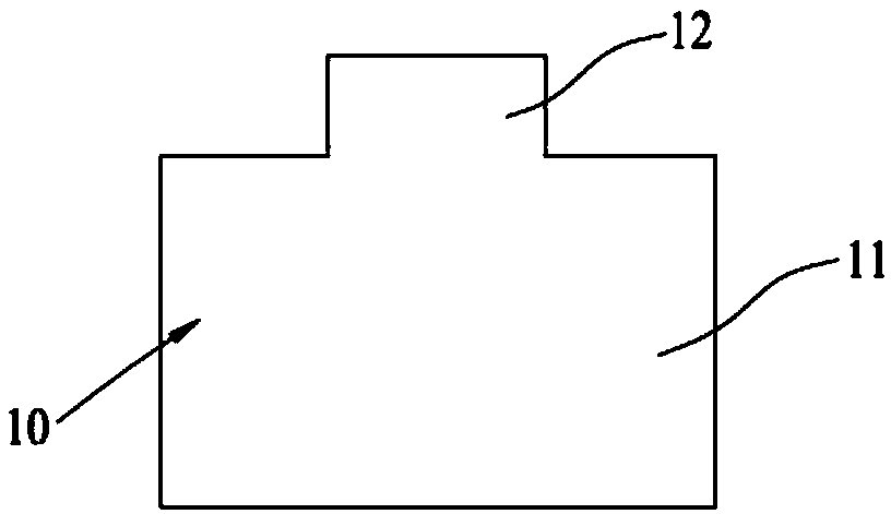
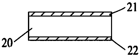
[0044] figure 1The structure of the heat dissipation substrate in Embodiment 1 is shown, the heat dissipation substrate includes an insulating base material 30, a metal conductive member 10 embedded in the insulating base material 30, and a ceramic heat dissipation member 20; in the thickness direction of the heat dissipation substrate, the ceramic heat dissipation The component 20 is located within the contour range of the metal conductive component 10 , and the thickness of the ceramic heat dissipation component 20 is smaller than that of the metal conductive component 10 . The metal conductive member 10 includes a metal body 11 and one or more bosses 12 extending upward from the metal body 11. The height of the bosses 12 (dimensions in the thickness direction of the heat dissipation substrate) is preferably 0.1 mm to 1 mm. In the example it is 0.4 mm. The thickness of the ceramic heat dissipation member 20 is preferably 0.2 mm to 0.8 mm, for example, 0.35 mm in this embodi...

Embodiment 2

[0060] The difference between embodiment 2 and embodiment 1 is only that: the metal conductive member 110 in embodiment 2 does not have an upwardly extending boss structure.

[0061] In other embodiments of the present invention, the heat dissipation substrate may also have an inner conductive circuit formed in the insulating substrate, and the inner conductive circuit may be electrically connected to the patterned conductive layer on the upper surface of the insulating substrate through conductive vias.


PUM

PropertyMeasurementUnit
heightaaaaaaaaaa
thicknessaaaaaaaaaa
thicknessaaaaaaaaaa

Abstract

The invention relates to a heat dissipation substrate and a preparation method thereof. The heat dissipation substrate comprises an insulating substrate, a metal conductive member embedded in the insulating substrate, a patterned conductive layer formed on the upper surface of the insulating substrate and a metal heat dissipation layer formed on the lower surface of the heat dissipation substrate.A power device mounting pad exposed to an insulating substrate is formed on an upper surface of the metal conductive member, and a ceramic heat conductive member is disposed between the metal conductive member and the metal heat dissipation layer. As that heat dissipation substrate can simultaneously carry power devices and non-power device, the heat dissipation substrate is convenient to realizeminiaturization, and has good heat dissipation performance and voltage withstand performance. The preparation method comprises the steps of molding an insulating substrate by hot pressing and embedding a metal conductive member and a ceramic heat dissipation member in the insulating substrate, the preparation process is simple and the cost is low.

Description

technical field [0001] The invention relates to a heat dissipation substrate and a preparation method thereof. Background technique [0002] Semiconductor power devices such as thyristors, GTOs (gate turn-off thyristors), GTRs (power transistors), IGBTs (insulated gate bipolar transistors), MOSFETs (power field effect transistors) and power diodes usually carry loads during operation. A large current generates a large amount of heat. In order to avoid heat accumulation to form high temperature and affect its performance, the heat generated by power semiconductor devices needs to be dissipated in time by the heat dissipation substrate as its electrical connection and mechanical bearing substrate. [0003] With the development of electronic / power products in the direction of light conversion and small conversion, more and more electronic / electric products are designed such as semiconductor power devices and non-power devices such as voltage stabilization / rectification / filter d...

Claims


Application Information

Patent Timeline
Patent Type & Authority Applications(China)
IPC IPC(8): H01L23/498H01L23/367H01L21/48
CPCH01L21/4857H01L21/486H01L21/4882H01L23/367H01L23/49822H01L23/49827
Inventor 袁绪彬高卫东梁可为林伟健
Owner RAYBEN TECH ZHUHAI
Why Eureka
Try Eureka