Pixel-defining structure and preparation method thereof, and OLED device

A technology of pixel definition and pixel definition layer, which is applied in the manufacture of electric solid-state devices, semiconductor devices, and semiconductor/solid-state devices, etc. Reduce coffee ring effect, avoid color mixing, and uniform film thickness

Inactive Publication Date: 2019-01-04
SHENZHEN CHINA STAR OPTOELECTRONICS TECH CO LTD
View PDF3 Cites 12 Cited by
  • Summary
  • Abstract
  • Description
  • Claims
  • Application Information

AI Technical Summary

Problems solved by technology

In the production process of the existing printed OLED, the pixel defining layer is a hydrophilic material, which will lead to uneven film thickness of the organic electroluminescent film, such as Figure 1a As shown, the pixel defining layer is a hydrophobic material, which will lead to edge leakage and uneven film thickness of the organic electroluminescent film, such as Figure 1b shown

Method used


Image

  • Pixel-defining structure and preparation method thereof, and OLED device
  • Pixel-defining structure and preparation method thereof, and OLED device
  • Pixel-defining structure and preparation method thereof, and OLED device

Examples


Embodiment Construction

[0027] Hereinafter, embodiments of the present invention will be described in detail with reference to the accompanying drawings. This invention may, however, be embodied in many different forms and should not be construed as limited to the specific embodiments set forth herein. Rather, the embodiments are provided to explain the principles of the invention and its practical application, thereby enabling others skilled in the art to understand the invention for various embodiments and with various modifications as are suited to particular intended uses. In the drawings, the same reference numerals will be used to denote the same elements throughout.

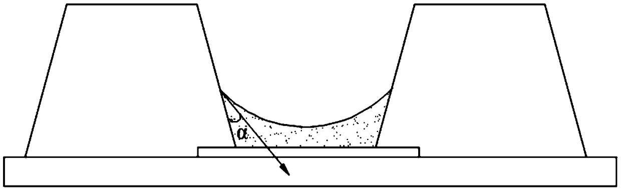
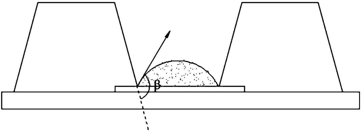
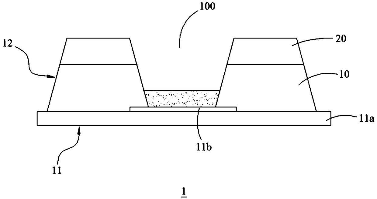
[0028] The pixel defining structure in this embodiment can be applied to OLED devices, and can also be applied to quantum dot light emitting (Quantum Dot Light Emitting Diodes, QLED) devices. The following uses the pixel defining structure applied to OLED devices as an example to describe the pixel of the present invention Defin...


PUM


Abstract

The invention provides a pixel-defining structure and a preparation method thereof, and an OLED device. The preparation method comprises the following steps: providing a substrate; forming a pixel defining film on the substrate by a composition process; performing surface treatment on the top of the pixel defining film to form a first pixel defining layer having hydrophilicity and a second pixel defining layer having hydrophobicity. In the pixel defining structure prepared by the preparation method provided by the inveniton, the first pixel defining layer of the pixel defining film has hydrophilicity, the second pixel defining layer is hydrophobic, such that the contact angle between the first pixel defining layer and the ink of the organic luminescent material is small, the contact anglebetween the second pixel defining layer and the ink of the organic luminescent material is large, so that the coffee ring effect can be reduced, an organic electroluminescent film with uniform film thickness can be formed, and since the second pixel defining layer has hydrophobicity, the ink of different organic luminescent materials can be prevented from flowing into adjacent pixel regions to cause color mixing, and the performance of the OLED device can be improved.

Description

technical field [0001] The invention relates to the technical field of organic electroluminescence diode display, in particular to a pixel defining structure, a preparation method thereof, and an OLED device. Background technique [0002] Organic Light Emitting Diode (OLED) has the characteristics of self-luminescence, bendability, wide viewing angle, long life, energy saving and environmental protection. The existing OLED types mainly include evaporation type and printing type. The cost of evaporation type OLED is relatively high, while the cost of printing type OLED is low and easy to be large-sized. Therefore, printing type OLED has attracted widespread attention in the industry. [0003] The key to the production of printed OLEDs is to accurately drop the organic light-emitting material ink into the pixel pits formed by the pixel defining layer, so as to obtain an organic electroluminescent film with uniform film thickness. In the production process of the existing prin...

Claims


Application Information

Patent Timeline
Patent Type & Authority Applications(China)
IPC IPC(8): H01L27/32H01L51/56
CPCH10K59/122H10K71/00
Inventor 周凯锋
Owner SHENZHEN CHINA STAR OPTOELECTRONICS TECH CO LTD
Why Eureka
Try Eureka