Semiconductor device and method of forming the same

A technology of semiconductors and devices, which is applied in the field of semiconductor devices and their formation, can solve the problems that the performance of semiconductor devices needs to be improved, and achieve the effect of improving shape consistency and improving reliability

Active Publication Date: 2021-07-13
SEMICON MFG INT (SHANGHAI) CORP +1
View PDF0 Cites 0 Cited by
  • Summary
  • Abstract
  • Description
  • Claims
  • Application Information

AI Technical Summary

Problems solved by technology

[0004] However, the performance of semiconductor devices composed of existing fin field effect transistors needs to be improved

Method used


Image

  • Semiconductor device and method of forming the same
  • Semiconductor device and method of forming the same
  • Semiconductor device and method of forming the same

Examples


Embodiment Construction

[0035] As mentioned in the background, the performance of semiconductor devices in the prior art is relatively poor.

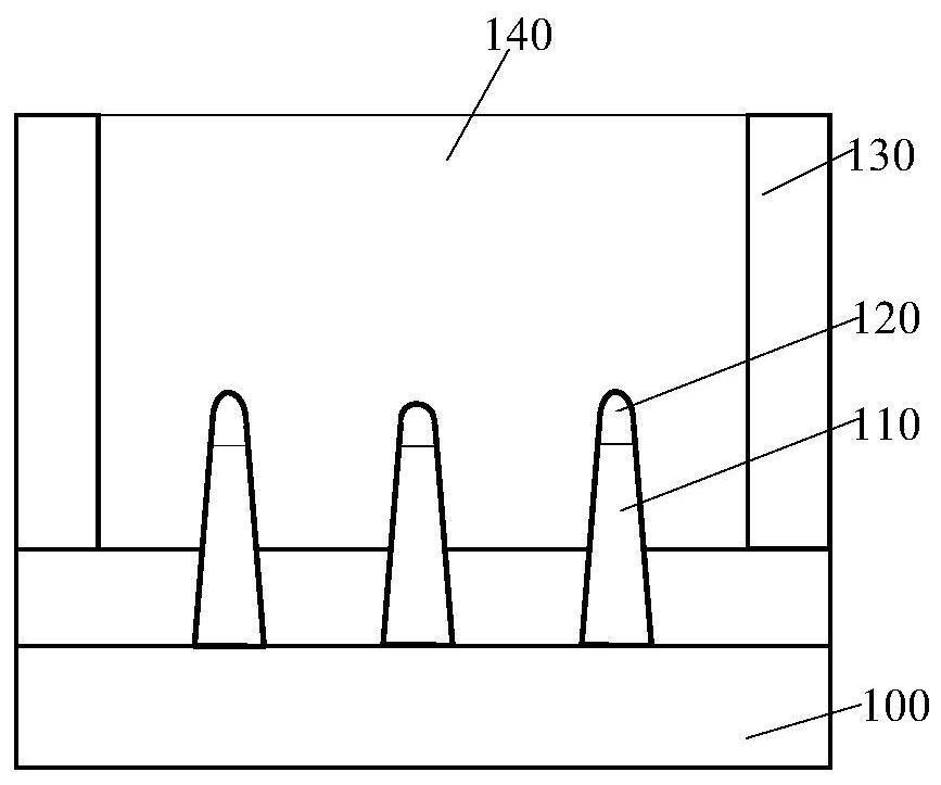
[0036] A method for forming a fin field effect transistor, referring to figure 1 , including: providing a base, the base includes a substrate 100 and several fins 110 on the substrate; forming a doped region 120, a gate structure and a dielectric layer 130 on the base, and the gate structure spans the several fins 110. Covering part of the top surface and part of the sidewall surface of the fin 110, the doped regions 120 are respectively located in the fins 110 on both sides of the gate structure, and the dielectric layer 130 covers the gate structure, the fin 110 and the doped region 120; Grooves (not shown) penetrating through the dielectric layer 130 are respectively formed in the dielectric layer 130 on both sides of the gate structure; source and drain plugs 140 are formed in the trenches, and the source and drain plugs 140 and the doped regions 120 top ...


PUM


Abstract

A semiconductor device and a method for forming the same, wherein the method includes: providing a substrate with several fins on the substrate; forming an initial doping region and a dielectric layer, the initial doping regions are respectively located in the several fins, and initially The doped region includes a bottom region and a top region located on the bottom region, the dielectric layer covers the fin, the initial doped region and the substrate; a trench penetrating through the dielectric layer is formed in the dielectric layer, and the initially doped region is located in the trench bottom, and the trench exposes the top region; etching removes the top region at the bottom of the trench, so that the bottom region forms a doped region. The method improves the shape consistency of the top surface of the doped region in different fins at the bottom of the groove, and improves the reliability of the semiconductor device.

Description

technical field [0001] The invention relates to the field of semiconductor manufacturing, in particular to a semiconductor device and a forming method thereof. Background technique [0002] MOS transistors are one of the most important components in modern integrated circuits. The basic structure of a MOS transistor includes: a semiconductor substrate; a gate structure located on the surface of the semiconductor substrate, a source region located in the semiconductor substrate on one side of the gate structure, and a drain region located in the semiconductor substrate on the other side of the gate structure. The working principle of the MOS transistor is: by applying a voltage to the gate structure, the current through the channel at the bottom of the gate structure is adjusted to generate a switching signal. [0003] With the development of semiconductor technology, the ability of the traditional planar MOS transistor to control the channel current becomes weaker, resultin...

Claims


Application Information

Patent Timeline
Patent Type & Authority Patents(China)
IPC IPC(8): H01L29/78H01L29/10H01L29/423H01L21/336
CPCH01L29/1025H01L29/42356H01L29/66795H01L29/7855
Inventor 张海洋刘盼盼
Owner SEMICON MFG INT (SHANGHAI) CORP
Why Eureka
Try Eureka