Silicon heterojunction solar cell and preparation method thereof

A solar cell and silicon heterojunction technology, applied in the field of solar cells, can solve the problems of reduced strength, easy oxidation and corrosion of Cu, and increased resistance, and achieve good oxidation resistance, improved environmental impact resistance and weldability.

Pending Publication Date: 2019-01-04
国家电投集团新能源科技有限公司
View PDF5 Cites 9 Cited by
  • Summary
  • Abstract
  • Description
  • Claims
  • Application Information

AI Technical Summary

Problems solved by technology

This electrode has thinner grid lines and lower contact resistance. However, in a humid environment, Cu is easily oxidized and corroded, which greatly increases the resistance and reduces the strength.

Method used


Image

  • Silicon heterojunction solar cell and preparation method thereof
  • Silicon heterojunction solar cell and preparation method thereof
  • Silicon heterojunction solar cell and preparation method thereof

Examples


Embodiment 1

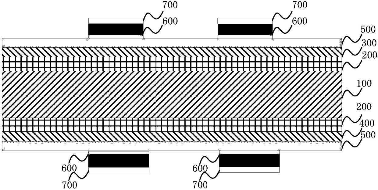
[0113] Prepare the main body layer of silicon heterojunction solar cells according to the following steps:

[0114] (1) An n-type crystalline silicon substrate 100 is provided, the n-type crystalline silicon substrate 100 is cleaned, and textured structures are formed on the upper surface and the lower surface.

[0115] (2) The n-type crystalline silicon substrate is placed in a hydrogen atmosphere for hydrogenation pretreatment.

[0116] (3) Deposit a lightly doped n-type hydrogenated amorphous silicon (a-Si:H) buffer layer on the upper and lower surfaces of the n-type crystalline silicon substrate 100, and the lightly doped n-type hydrogenated amorphous silicon layer uses phosphorus (P ) as the doping element, the doping concentration is 10 14 / cm 3 , with a thickness of 6nm.

[0117] (4) Deposit a heavily doped p-type a-Si:H emitter layer on the surface of the lightly doped n-type hydrogenated amorphous silicon (a-Si:H) buffer layer located on the upper surface, the heav...

Embodiment 2

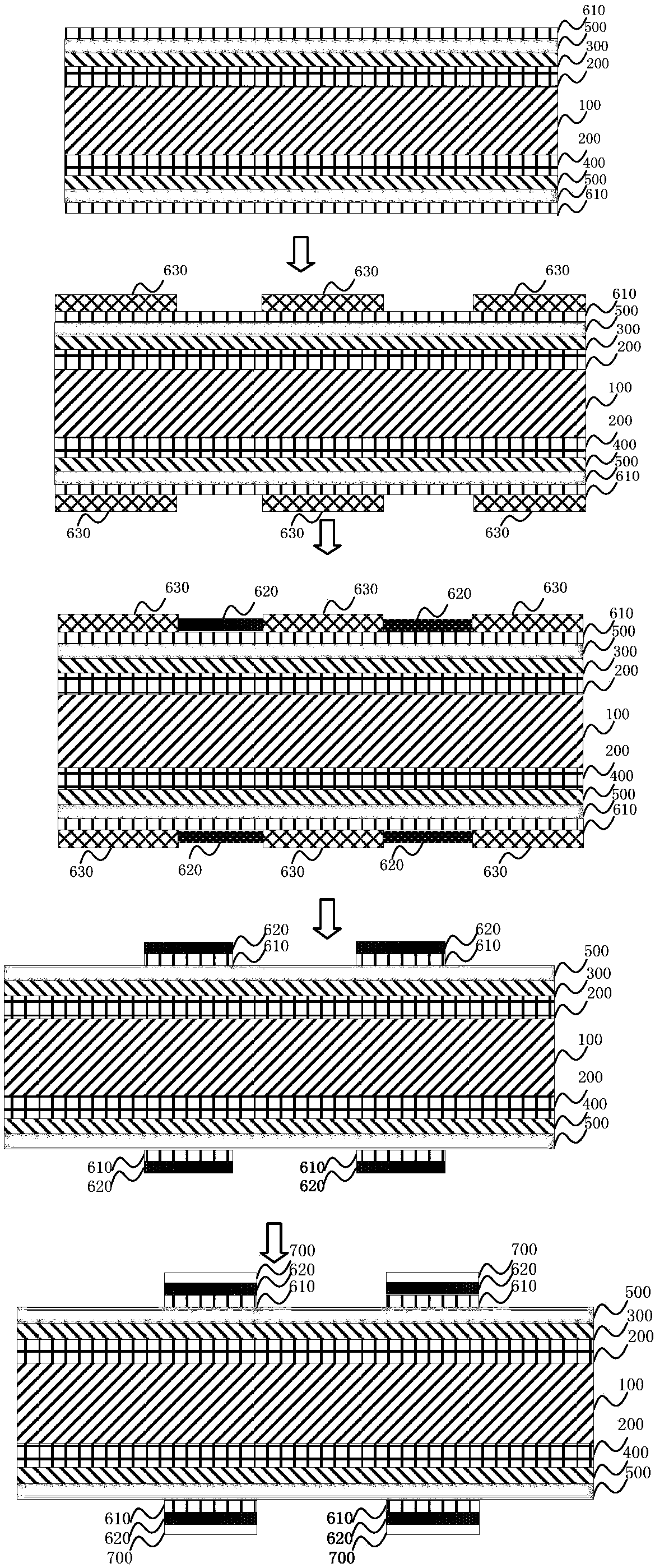
[0122] refer to image 3 , the steps of preparing a silicon heterojunction solar cell using the method for preparing a solar cell according to an embodiment of the present invention are as follows:

[0123] (1) A Ti-Al alloy transition layer 610 with a thickness of 20 nm was formed on the surface of the transparent conductive oxide of the main body layer prepared in Example 1 by magnetron sputtering.

[0124] (2) Form a photoresist film 630 on the surface of the Ti-Al alloy transition layer 610 by spin coating, and heat and dry to form a dry film.

[0125] (3) using a mask plate with an electrode pattern and a photolithography method to open holes at the position where the predetermined electrode pattern is formed on the dry film.

[0126] (4) Form a Cu metal layer 620 with a thickness of 30 μm at the opening of the dry film by electroplating. The dry film is electrically insulated, so the part outside the opening will not be plated with Cu.

[0127] (5) Remove the dry film ...

Embodiment 3

[0131] refer to Figure 4 , the steps of preparing a silicon heterojunction solar cell using the method for preparing a solar cell according to an embodiment of the present invention are as follows:

[0132] (1) A Ti-Al alloy transition layer 610 with a thickness of 20 nm was formed on the surface of the transparent conductive oxide of the main body layer prepared in Example 1 by magnetron sputtering.

[0133] (2) Form a photoresist film 630 on the surface of the Ti-Al alloy transition layer 610 by spin coating, and heat and dry to form a dry film.

[0134] (3) using a mask plate with an electrode pattern and a photolithography method to open holes at the position where the predetermined electrode pattern is formed on the dry film.

[0135] (4) Form a Cu metal layer 620 with a thickness of 30 μm at the opening of the dry film by electroplating. The dry film is electrically insulated, so the part outside the opening will not be plated with Cu.

[0136] (5) The second electrop...


PUM

PropertyMeasurementUnit
thicknessaaaaaaaaaa
thicknessaaaaaaaaaa
thicknessaaaaaaaaaa

Abstract

The invention discloses a silicon heterojunction solar cell and a preparation method thereof. Wherein the solar cell comprises an n-type crystalline silicon substrate layer; a lightly doped an n-typehydrogenated amorphous silicon buffer layer formed on the upper and lower side surfaces of the substrate layer; a heavily doped p-type hydrogenated amorphous silicon emitter layer formed on the surface of one side of lightly doped n-type hydrogenated amorphous silicon buffer layer; a heavily doped n-type hydrogenated amorphous silicon back field layer formed on the surface of the other side of thehydrogenated amorphous silicon buffer layer; transparent conductive oxide layers formed on the surfaces of the hydrogenated amorphous silicon emitter layer and the hydrogenated amorphous silicon backfield layer, respectively; an alloy gate line electrode layer formed on a surface of at least one of the transparent conductive oxide layer, hydrogenated amorphous silicon back field layer, and hydrogenated amorphous silicon emitter layer; and an electrode protection layer formed on the surface of the alloy gate line electrode layer.

Description

technical field [0001] The invention relates to the field of solar cells, in particular to a silicon heterojunction solar cell containing an alloy electrode protective layer and a preparation method thereof. Background technique [0002] The electrodes of photovoltaic cells are usually located on the front or back surface of the cell, forming close physical or chemical contact with the cell surface, and serving as conductors for collecting the photo-generated current generated by the cell. Electrodes, also known as grid lines, are distributed on the surface of photovoltaic cells in a certain arrangement pattern, the purpose is to provide a low-resistance conductive path, and minimize the shielding of light by the electrodes themselves to reduce the loss of incident light. [0003] The metal electrodes on the surface of solar cells not only affect the series resistance of the battery, and then affect the efficiency of the final battery, but also affect the cost of the battery...

Claims


Application Information

Patent Timeline
Patent Type & Authority Applications(China)
IPC IPC(8): H01L31/0224H01L31/074H01L31/18
CPCH01L31/022425H01L31/074H01L31/18Y02E10/50Y02P70/50
Inventor 赵晓霞王恩宇王伟田宏波周永谋杨瑞鹏宗军李洋
Owner 国家电投集团新能源科技有限公司
Why Eureka
Try Eureka