A technology for bon a dual-row QFN integrated circuit

An integrated circuit and welding process technology, which is applied in the field of double-row QFN integrated circuit welding process, can solve problems such as increasing risks, and achieve the effects of increasing tin climbing height, reducing volume, and solving virtual soldering

Inactive Publication Date: 2019-01-04
成都京蓉伟业电子有限公司
View PDF3 Cites 2 Cited by
  • Summary
  • Abstract
  • Description
  • Claims
  • Application Information

AI Technical Summary

Problems solved by technology

The judgment can only be checked in the final functional test, which greatly increases the risk

Method used


Image

  • A technology for bon a dual-row QFN integrated circuit
  • A technology for bon a dual-row QFN integrated circuit
  • A technology for bon a dual-row QFN integrated circuit

Examples


Embodiment 1

[0027] A double-row QFN integrated circuit welding process is characterized in that it comprises the following process steps:

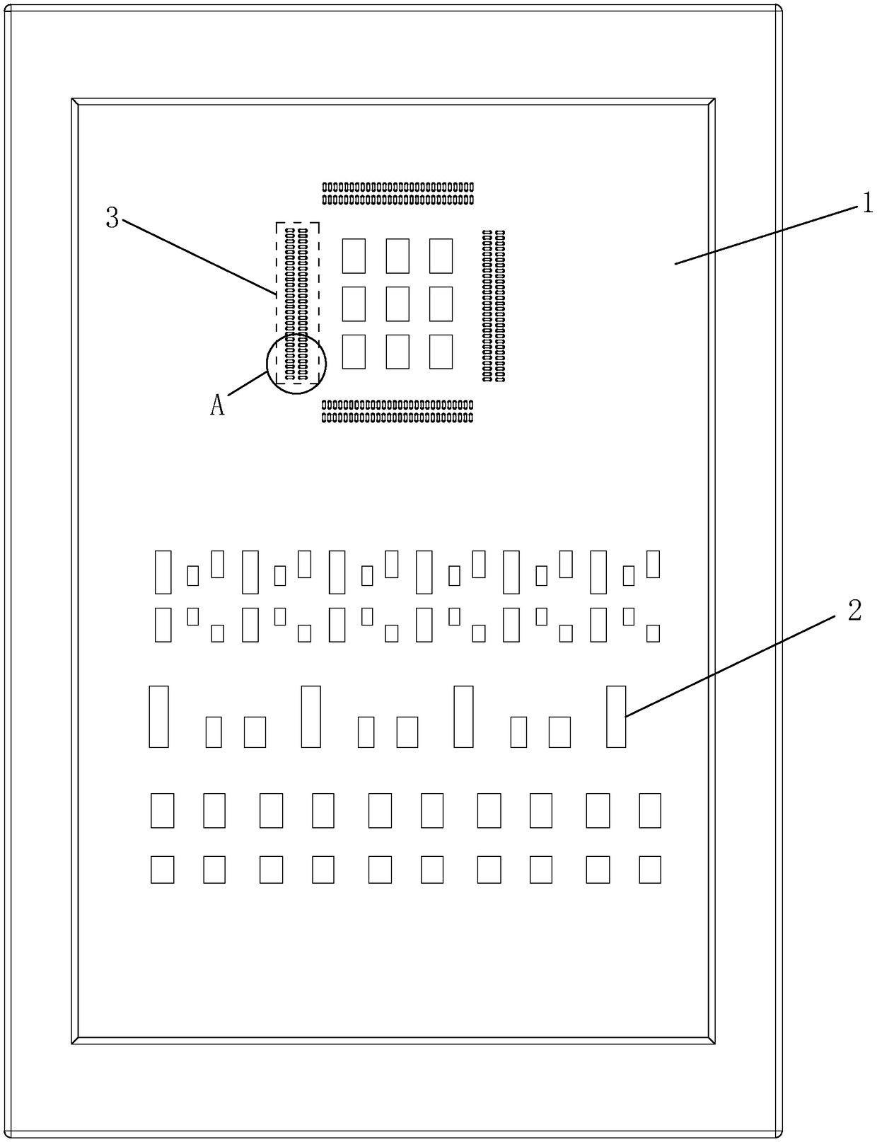
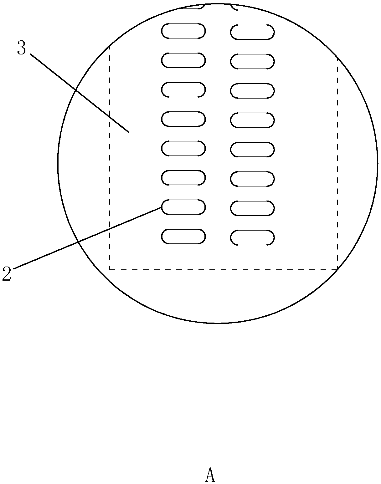
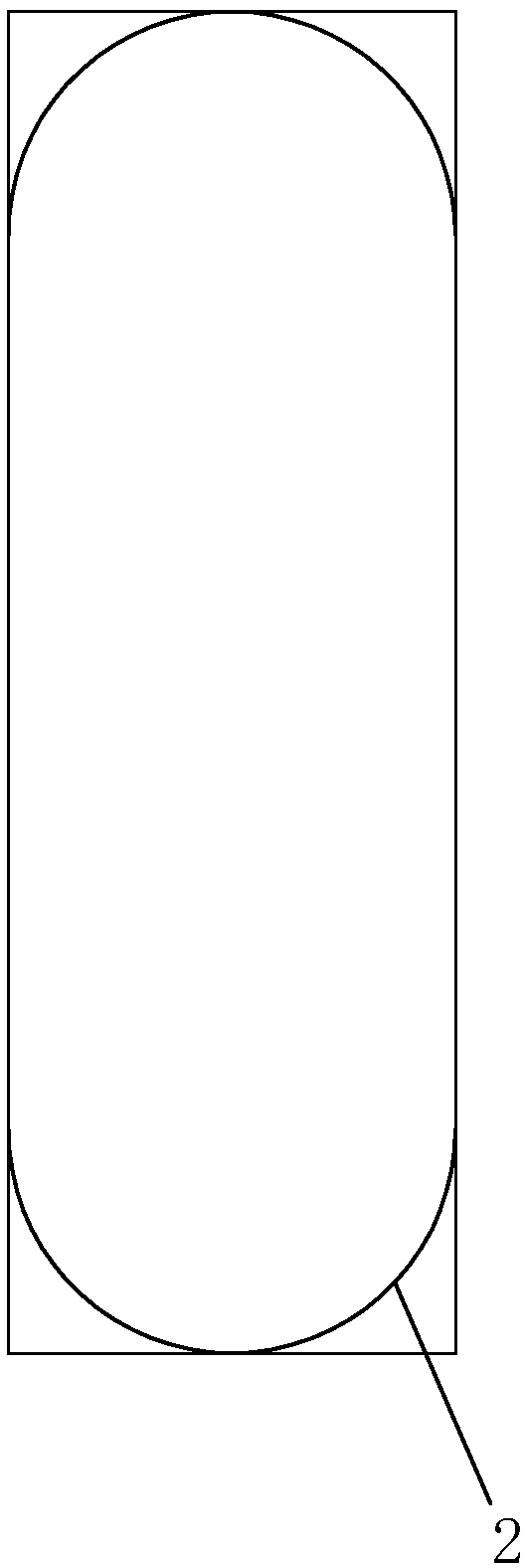
[0028] S1) Screen printing: Use a screen printing machine to brush solder paste on the pads of the circuit board, wherein the area where the distance between the openings 2 on the steel plate 1 is less than or equal to 0.2mm is set as the fine-pitch area 3, and the fine-pitch area The ratio of the area of ​​the opening 2 in 3 to the area of ​​the circuit board pad is 0.85, the opening 2 in the fine-pitch area 3 is waist-shaped, and the two long sides of the opening 2 in the fine-pitch area 3 are straight lines parallel to each other And the two ends of the length direction of the opening 2 are symmetrical circular arcs, the thickness of the steel plate 1 is 0.09mm, the thickness ratio of the thickness of the fine-pitch area 3 to the thickness of the steel plate 1 is 0.85; the printing speed of the screen printing machine is 30mm / s, The front and rear ...

Embodiment 2

[0035] A double-row QFN integrated circuit welding process is characterized in that it comprises the following process steps:

[0036] S1) Screen printing: Use a screen printing machine to brush solder paste on the pads of the circuit board, wherein the area where the distance between the openings 2 on the steel plate 1 is less than or equal to 0.2mm is set as the fine-pitch area 3, and the fine-pitch area The ratio of the area of ​​the opening 2 in 3 to the area of ​​the circuit board pad is 0.9, the opening 2 in the fine-pitch area 3 is waist-shaped, and the two long sides of the opening 2 in the fine-pitch area 3 are straight lines parallel to each other And the two ends of the length direction of the opening 2 are symmetrical circular arcs, the thickness of the steel plate 1 is 0.1mm, and the thickness ratio of the thickness of the fine-pitch area 3 to the thickness of the steel plate 1 is 0.9; the printing speed of the screen printing machine is 36mm / s, The front and rear...

Embodiment 3

[0043] A double-row QFN integrated circuit welding process is characterized in that it comprises the following process steps:

[0044] S1) Screen printing: Use a screen printing machine to brush solder paste on the pads of the circuit board, wherein the area where the distance between the openings 2 on the steel plate 1 is less than or equal to 0.2mm is set as the fine-pitch area 3, and the fine-pitch area The ratio of the area of ​​the opening 2 in 3 to the area of ​​the circuit board pad is 0.95, the opening 2 in the fine-pitch area 3 is waist-shaped, and the two long sides of the opening 2 in the fine-pitch area 3 are straight lines parallel to each other And the two ends of the length direction of the opening 2 are symmetrical circular arcs, the thickness of the steel plate 1 is 0.11mm, the thickness ratio of the thickness of the fine-pitch area 3 to the thickness of the steel plate 1 is 0.95; the printing speed of the screen printing machine is 40mm / s, The front and rear ...


PUM


Abstract

The invention relates to a welding process of a dual-row QFN integrated circuit, Circuit board weld field, The process comprises the following steps: S1) screen printing: brushing solder paste on thebonding pad of the circuit board by a screen printer, wherein the ratio of the area of the aperture in the fine pitch area to the area of the bonding pad of the circuit board is 0.85 to 0.95, the thickness of the steel plate is 0.09 to 0.11 mm, and the ratio of the thickness of the fine pitch area to the thickness of the steel plate is 0.85 to 0.95; The printing speed of screen printer is 30-40mm/s, the pressure of front and back scraper is 2.5-3.5 kg, the demoulding length is 1.4-1.6 mm, and the demoulding speed is 0.4-0.6 mm/s. 2) mount: mounting with a mount machine; S3) reflow soldering: reflow soldering is carried out by using a reflow soldering equipment, wherein the temperature peak value of the reflow soldering is 240 +/- 5 DEG C, the reflow time when the temperature is higher than217 DEG C is 30 to 60 seconds, and the temperature rise slope is less than or equal to 3 DEG C/s; S4) testing: testing the soldering quality and assembly quality of the assembled circuit board; S5) repairing: repairing the circuit board which is detected to be out of order, so as to improve the qualification rate of the double-row QFN integrated circuit.

Description

technical field [0001] The invention relates to the technical field of circuit board welding, in particular to a double-row QFN integrated circuit welding process. Background technique [0002] With the advent of the Internet of Things era, the development of communication technology can be said to be advancing thousands of miles. Often integrated circuit packaging and testing technology as the first and must lead the communication products. The packaging of integrated circuits, especially the development and packaging and testing of central processing units is a pioneer among pioneers. The central processing unit using double-row QFN packaging technology came into being. For the SMT welding process, it poses a great challenge. First of all, compared with single-row QFN, double-row QFN has more pins within one week, and its spacing is only 0.2 mm, which is prone to soldering. After soldering, it is impossible to judge whether the soldering is good with the naked eye. the...

Claims


Application Information

Patent Timeline
Patent Type & Authority Applications(China)
IPC IPC(8): H05K3/12H05K3/34
CPCH05K3/1216H05K3/1225H05K3/341H05K3/3463H05K3/3489
Inventor 王皓
Owner 成都京蓉伟业电子有限公司
Why Eureka
Try Eureka