A semiconductor laser having an inverse waveguide layer structure and a manufacturing method thereof

A technology of anti-waveguide and laser, which is applied in the direction of semiconductor lasers, optical waveguide semiconductor structures, lasers, etc., can solve the problems of complex implementation and high cost, and achieve the effects of low cost and processing difficulty, improved efficiency and power, and high beam quality

Inactive Publication Date: 2019-01-11
INST OF APPLIED ELECTRONICS CHINA ACAD OF ENG PHYSICS
View PDF5 Cites 1 Cited by
  • Summary
  • Abstract
  • Description
  • Claims
  • Application Information

AI Technical Summary

Problems solved by technology

Although the above methods can improve the beam quality and laser brightness to a certain extent, these methods have the defects of high cost and complicated implementation to varying degrees.

Method used


Image

  • A semiconductor laser having an inverse waveguide layer structure and a manufacturing method thereof
  • A semiconductor laser having an inverse waveguide layer structure and a manufacturing method thereof

Examples


Embodiment

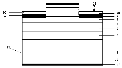
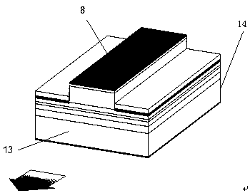
[0037] Embodiment: the embodiment of the present invention is such as figure 1 , figure 2 As shown, taking a wide-strip semiconductor laser as an example, the method for preparing a semiconductor laser with an anti-waveguide layer structure includes the following steps:

[0038] 1. Sequentially epitaxially grow the semiconductor laser structure on the substrate (1), including: lower confinement layer (2), lower waveguide layer (3), quantum well layer (4), upper waveguide layer (5), upper confinement layer ( 6), the upper metallization layer (7).

[0039] 2. Carry out the first photolithography on the substrate to fabricate the strip-shaped oscillating region (8), and the fabricating method is dry etching or wet etching. The etching depth is within the range of the upper waveguide layer (5) and the upper confinement layer (6), preferably near the junction of the upper waveguide layer and the upper confinement layer, and the maximum etching depth is controlled not to exceed t...


PUM


Abstract

The invention provides a semiconductor laser with an inverse waveguide layer and a manufacturing method thereof. The method comprises the following steps: a substrate, an epitaxial layer, a side opposite waveguide layer, a front cavity surface and a back cavity surface; an epitaxial layer is arranged on the top surface of the substrate. The front cavity surface is arranged on one side of the substrate. The rear cavity surface is arranged on the substrate side of the front cavity face side. The epitaxial layer is provided with a convex strip-shaped oscillation region; at least one side of the two sides of the strip-shaped oscillation region is provided with an inverse waveguide layer. An inverse waveguide layer is disposed on the epitaxial layer. This scheme can suppress the high-order modebetter than the existing mode control technology on both sides of the oscillation region, so as to improve the beam quality and enhance the brightness of the semiconductor laser.

Description

technical field [0001] The invention relates to the field of design and manufacture of semiconductor lasers, in particular to a semiconductor laser with an anti-waveguide layer and a manufacturing method thereof. Background technique [0002] Semiconductor lasers have the advantages of high electro-optical efficiency, small size, and high reliability, and have important applications in the fields of pumping solid-state lasers, industrial processing, medical treatment, and space communications. With the emergence of new application scenarios such as pumping high-brightness fiber lasers and spectral synthesis, higher requirements are put forward for new high-brightness semiconductor lasers with high power and high beam quality characteristics. For the most commonly used semiconductor lasers with a wide light-emitting area, the difficulty in improving brightness lies in: although the power is high (10-25W), affected by factors such as high-order modes and filamentary luminescen...

Claims


Application Information

Patent Timeline
Patent Type & Authority Applications(China)
IPC IPC(8): H01S5/34H01S5/20
CPCH01S5/205H01S5/34
Inventor 李弋周坤杜维川康俊杰高松信武德勇胡耀张亮
Owner INST OF APPLIED ELECTRONICS CHINA ACAD OF ENG PHYSICS
Why Eureka
Try Eureka