A method of making a memory
A manufacturing method and memory technology, applied in semiconductor/solid-state device manufacturing, semiconductor devices, electric solid-state devices, etc., can solve the problems of charge capture, damage, over-etching, etc., to improve performance, increase package area, and increase coupling rate Effect
- Summary
- Abstract
- Description
- Claims
- Application Information
AI Technical Summary
Problems solved by technology
Method used
Image
Examples
Embodiment Construction
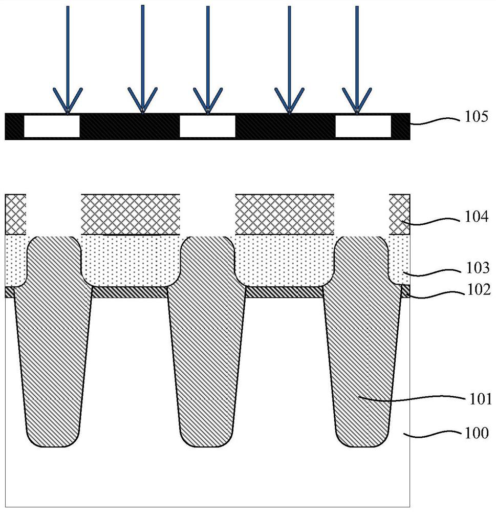
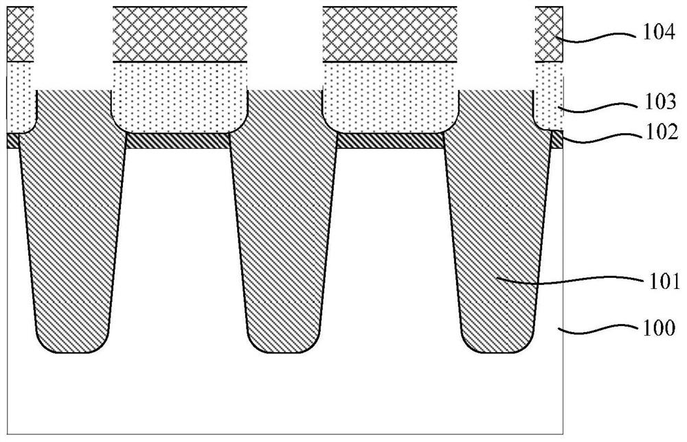
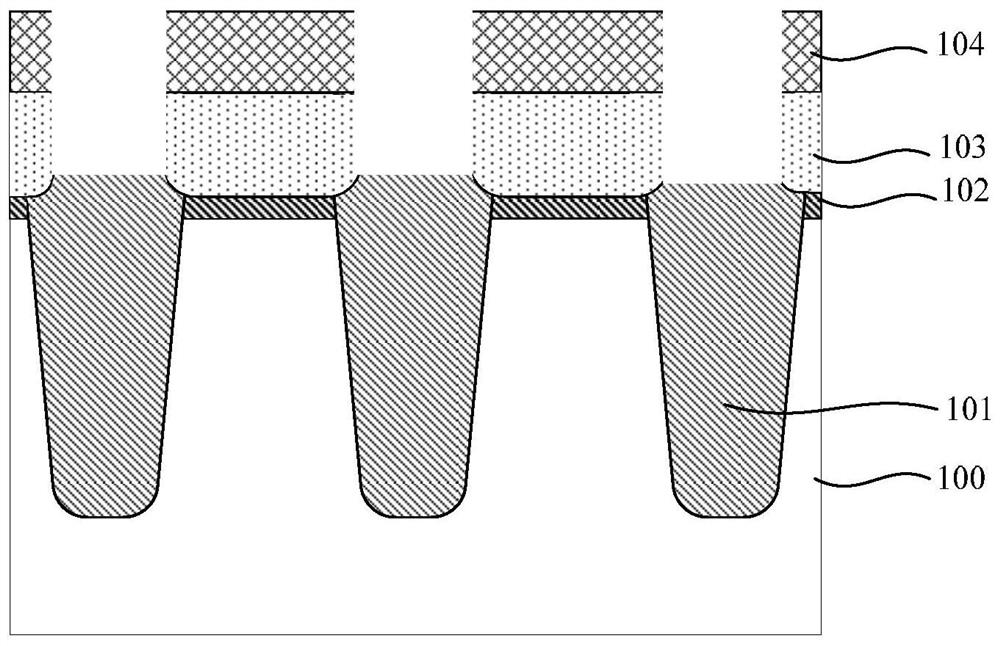
[0028] As mentioned in the background art, after the floating gates are formed in the memory manufacturing process, the isolation structure between adjacent floating gates will be etched to form trenches of required depth, thereby exposing the sidewalls of the floating gates, increasing the gate The wrapping area of the interlayer (ONO) and the control gate to the floating gate improves the coupling rate. The etching of the isolation structure generally adopts a wet etching process. Due to the isotropy of the wet etching, while ensuring the etching depth of the trench, it is easy to cause over-etching, that is, the wet etching solution is easy to corrode. Tunneling oxide at the bottom of the floating gate. If dry etching (anisotropic etching) is used, although there will be no over-etching phenomenon, due to the limitations of dry etching, the floating gate will be damaged or trapped under the action of plasma. charge, which affects the performance of the floating gate.
...
PUM
 Abstract
Description
Claims
Application Information
 - R&D
- Intellectual Property
- Life Sciences
- Materials
- Tech Scout
- Unparalleled Data Quality
- Higher Quality Content
- 60% Fewer Hallucinations
Browse by: Latest US Patents, China's latest patents, Technical Efficacy Thesaurus, Application Domain, Technology Topic, Popular Technical Reports.
© 2025 PatSnap. All rights reserved.Legal|Privacy policy|Modern Slavery Act Transparency Statement|Sitemap|About US| Contact US: help@patsnap.com


