Gallium nitride-based light emitting diode epitaxial wafer and a manufacturing method thereof

A light-emitting diode, gallium nitride-based technology, applied in the direction of electrical components, circuits, semiconductor devices, etc., can solve problems affecting LED applications, poor current lateral expansion, etc., to improve horizontal expansion capabilities, reduce series resistance, and reduce forward The effect of voltage

Active Publication Date: 2019-01-22
HC SEMITEK ZHEJIANG CO LTD
View PDF2 Cites 7 Cited by
  • Summary
  • Abstract
  • Description
  • Claims
  • Application Information

AI Technical Summary

Problems solved by technology

[0006] The embodiment of the present invention provides a gallium nitride-based light-emitting diode epitaxial wafer and its manufacturing method, which can solve the problem of poor lateral expansion of current in the P-type semiconductor layer in the prior art, which affects the application of LEDs in civil lighting.

Method used


Image

  • Gallium nitride-based light emitting diode epitaxial wafer and a manufacturing method thereof
  • Gallium nitride-based light emitting diode epitaxial wafer and a manufacturing method thereof
  • Gallium nitride-based light emitting diode epitaxial wafer and a manufacturing method thereof

Examples


Embodiment Construction

[0026] In order to make the object, technical solution and advantages of the present invention clearer, the implementation manner of the present invention will be further described in detail below in conjunction with the accompanying drawings.

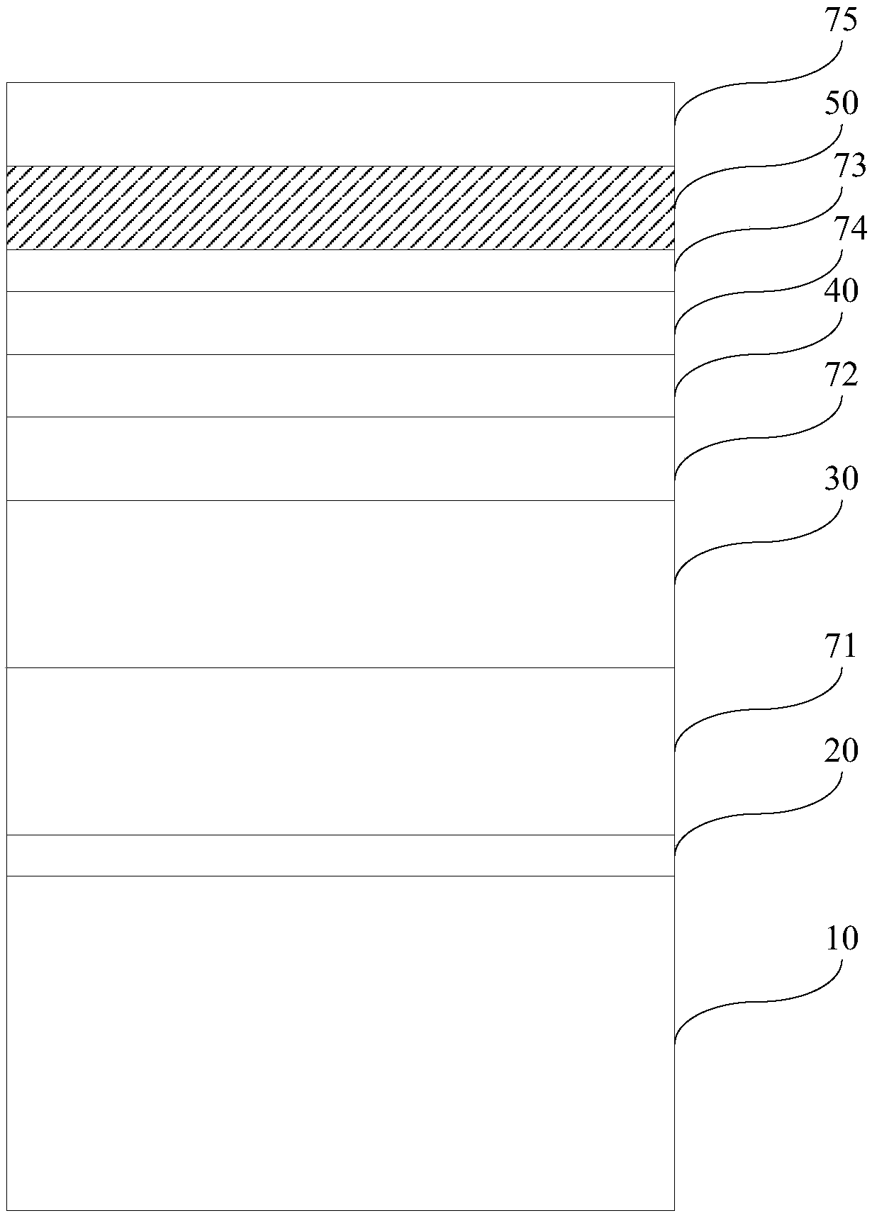
[0027] An embodiment of the present invention provides a GaN-based light-emitting diode epitaxial wafer, figure 1 For a structural schematic diagram of a gallium nitride-based light-emitting diode epitaxial wafer provided in an embodiment of the present invention, see figure 1 , the GaN-based light-emitting diode epitaxial wafer includes a substrate 10, a buffer layer 20, an N-type semiconductor layer 30, an active layer 40, and a P-type semiconductor layer 50, and the buffer layer 20, the N-type semiconductor layer 30, and the active layer 40 and a P-type semiconductor layer 50 are sequentially stacked on the substrate 10 .

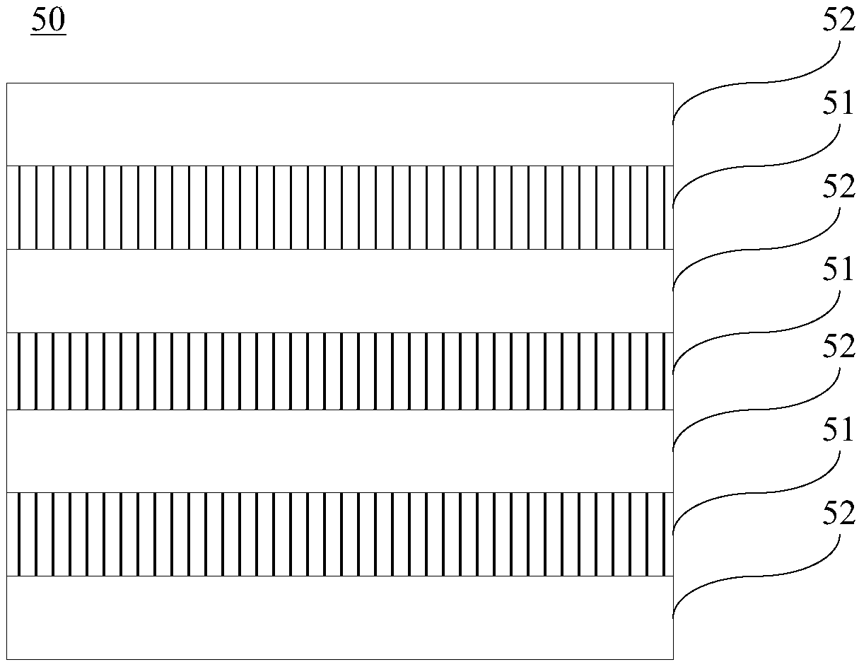
[0028] figure 2 For the schematic structural diagram of the P-type semiconductor layer provided by the embo...


PUM


Abstract

The invention discloses a gallium nitride-based light emitting diode epitaxial wafer and a manufacturing method thereof, belonging to the field of semiconductor technology. An epitaxial wafer includesa substrate, a buffer layer, an N-type semiconductor layer, an active layer and a P-type semiconductor layer. the buffer layer, the N-type semiconductor layer, the active layer and the P-type semiconductor layer are orderly stacked on the substrate. The P-type semiconductor layer comprises M undoped scandium aluminum nitride layers and (M+1) P-type doped gallium nitride layers. The M scandium aluminum nitride layers and the (M+1) gallium nitride layers are alternately laminated, and M is a positive integer. At least one undoped scandium aluminum nitride layer is inserted into the p-type dopedgallium nitride layer, The interface between scandium aluminum nitride layer and gallium nitride layer has strong two-dimensional hole gas, which can effectively improve the lateral expansion abilityof holes in the P-type semiconductor layer, reduce the series resistance of LED, and further reduce the forward voltage of LED, which is conducive to the application of LED in civil lighting.

Description

technical field [0001] The invention relates to the technical field of semiconductors, in particular to a gallium nitride-based light-emitting diode epitaxial wafer and a manufacturing method thereof. Background technique [0002] A light-emitting diode (English: Light Emitting Diode, referred to as: LED) is a semiconductor electronic component that can emit light. LED has the advantages of energy saving and environmental protection, high reliability, long service life, etc., so it has received widespread attention. In recent years, it has shined in the fields of backlight and display screens, and has begun to enter the civilian lighting market. For civilian lighting, power saving and durability are two important criteria, so reducing the series resistance of LEDs and improving the antistatic ability of LEDs are particularly critical. [0003] Gallium nitride (GaN) has good thermal conductivity, and has excellent characteristics such as high temperature resistance, acid and...

Claims


Application Information

Patent Timeline
Patent Type & Authority Applications(China)
IPC IPC(8): H01L33/14H01L33/00
CPCH01L33/007H01L33/14
Inventor 葛永晖郭炳磊王群吕蒙普胡加辉李鹏
Owner HC SEMITEK ZHEJIANG CO LTD
Why Eureka
Try Eureka