Microstructure surface liquid transport device for elastomer with electric field response performance and preparation method thereof

A technology of structural surface and electric field response, applied in applications, flat products, and other household appliances, can solve the problems of poor flexibility and controllability, and achieve the effect of simple operation, good reversibility, and fast response

Active Publication Date: 2019-01-29
BEIHANG UNIV
View PDF5 Cites 5 Cited by
  • Summary
  • Abstract
  • Description
  • Claims
  • Application Information

AI Technical Summary

Problems solved by technology
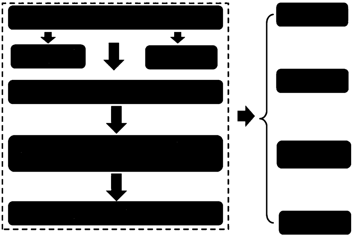
However, the current control methods for mechanical stretching of flexible substrates have poor flexibility and controllability, and are difficult to combine with practical applications.

Method used


Image

  • Microstructure surface liquid transport device for elastomer with electric field response performance and preparation method thereof
  • Microstructure surface liquid transport device for elastomer with electric field response performance and preparation method thereof
  • Microstructure surface liquid transport device for elastomer with electric field response performance and preparation method thereof

Examples


Embodiment 1

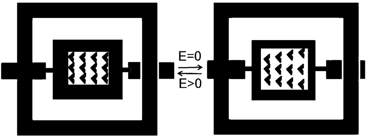
[0028] A PDMS film with anisotropic wetting properties includes a substrate and the micro-nano material, the substrate is an elastomer with electrical response properties, and the specific substrate is Dow Corning 184 polydimethylsiloxane.

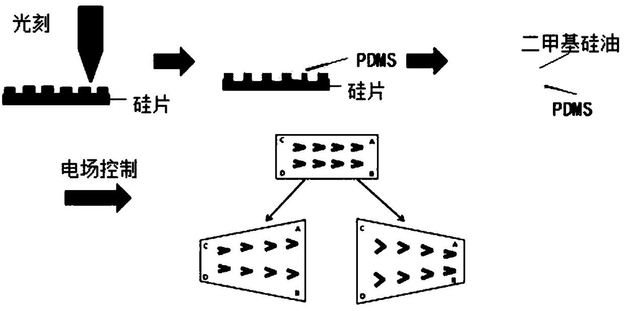
[0029] A method for preparing an anisotropic micro-nano structured surface material, comprising the following steps:

[0030] Step 1: Coat a layer of photoresist on the silicon wafer, use photolithography to carve the required "V" structure on the silicon wafer, and make different horizontal and vertical spacing;

[0031] Step 2: Select an elastomer with electrical response properties and mix it evenly with a ratio of 10:1 between the main agent and the curing agent;

[0032] Step 3: Remove air bubbles by vacuuming, place in an electric blast drying oven at 80°C-120°C for 1 hour, and then solidify and form;

[0033] Step 4: Take it out to cool down, and remove the PDMS film from the silicon wafer to obtain a structured PDMS film.

[0034...

Embodiment 2

[0041] A PDMS film with anisotropic wetting properties, including a substrate and the micro-nano material, the substrate is an elastomer with electrical response properties, and the substrate is selected from Dow Corning 184 polydimethylsiloxane, acrylate elastomer, polyurethane Any type of elastomer.

[0042] A method for preparing an anisotropic micro-nano structured surface material, comprising the following steps:

[0043] Step 1: Carve out the required asymmetric structure on the silicon wafer by designing the template, and make different horizontal and vertical spacings. The asymmetric structure is a trapezoidal prism;

[0044] Step 2: Select an elastomer with electrical response properties and mix it uniformly at a ratio of 10:1;

[0045]Step 3: Remove air bubbles by vacuuming, place in an electric blast drying oven at 80°C for 45 minutes, and then solidify and form;

[0046] Step 4: Take it out to cool down, and remove the PDMS film from the silicon wafer to obtain a...

Embodiment 3

[0054] A PDMS film with anisotropic wetting properties, including a substrate and the micro-nano material, the substrate is an elastomer with electrical response properties, and the substrate is selected from Dow Corning 184 polydimethylsiloxane, acrylate elastomer, polyurethane Any type of elastomer.

[0055] A method for preparing an anisotropic micro-nano structured surface material, comprising the following steps:

[0056] Step 1: Carve out the required asymmetric structure on the silicon wafer by designing the template, and make different horizontal and vertical spacings. The asymmetric structure is a trapezoidal prism;

[0057] Step 2: Select an elastomer with electrical response properties and mix it uniformly at a ratio of 10:1;

[0058] Step 3: Remove air bubbles by vacuuming, place in an electric blast drying oven at 80°C for 1 hour, and then solidify and form;

[0059] Step 4: Take it out to cool down, and remove the PDMS film from the silicon wafer to obtain a st...


PUM

PropertyMeasurementUnit
thicknessaaaaaaaaaa

Abstract

The invention discloses a microstructure surface liquid transport device for elastomer with electric field response performance, and further discloses a liquid transportation method. The microstructure surface liquid transport device comprises a substrate and micro-nanometer materials, wherein the substrate is the elastomer with electric response performance and is selected from any one of Dow Corning 184 polydimethylsiloxane, acrylate elastomer and polyurethane elastomer. A V-shaped prism with a V-shaped structure on the surface of the elastomer substrate is obtained through a conformal coating method; the elastomer substrate with the V-shaped structure is asymmetrically stretched by using an electric field; a driving force is generated by using an asymmetric Laplace pressure difference;and continuous and rapid transportation of liquid drops is realized by continuously repeating the process.

Description

technical field [0001] The invention relates to the field of electric field-induced dielectric elastomer microstructure surface-driven liquid transport, and more specifically relates to a device, preparation method and application for controlling the asymmetric change of surface structure and wettability by electric field-responsive micro-nano materials. Background technique [0002] External field-responsive wettable materials have broad application prospects in liquid transportation, anti-fog and anti-icing, and preparation of microreactors. [0003] At present, studies have shown that surface structure or composition gradients can be achieved through light, electricity, magnetism, external forces, etc., and then surface wettability gradients can be realized, and liquid droplets can be oriented to move, and then applied to liquid transport. The construction of micro-nano structures on the surface greatly increases the hydrophobicity of the surface (see reference [1] Y. Zhe...

Claims


Application Information

Patent Timeline
Patent Type & Authority Applications(China)
IPC IPC(8): B29C41/50B29C41/30B29L7/00B29K83/00
CPCB29C41/003B29C41/30B29C41/50B29K2083/00B29L2007/00
Inventor 田东亮李燕张孝芳刘克松江雷
Owner BEIHANG UNIV
Why Eureka
Try Eureka