Fin transistor and formation method thereof

A fin transistor and fin technology, which is applied in the fields of semiconductor devices, semiconductor/solid-state device manufacturing, electrical components, etc., can solve the problem of poor performance of fin field effect transistors, increased difficulty in the manufacturing process of fin field effect transistors, and improved reliability. to improve heat transfer, improve self-heating effect, and improve electrical performance

Active Publication Date: 2019-01-29
SEMICON MFG INT (SHANGHAI) CORP +1
View PDF4 Cites 5 Cited by
  • Summary
  • Abstract
  • Description
  • Claims
  • Application Information

AI Technical Summary

Problems solved by technology

[0004] However, as the density of semiconductor devices increases and the size shrinks, the manufacturing process of fin field eff

Method used


Image

  • Fin transistor and formation method thereof
  • Fin transistor and formation method thereof
  • Fin transistor and formation method thereof

Examples


Embodiment Construction

[0032] As described in the background art, as the density and size of semiconductor devices are increased, the performance of the formed fin field effect transistor is deteriorated, and the reliability thereof is reduced.

[0033] As the integration level of semiconductor devices increases, the self-heating effect seriously affects the reliability and service life of transistors. The following description will be made with reference to the accompanying drawings.

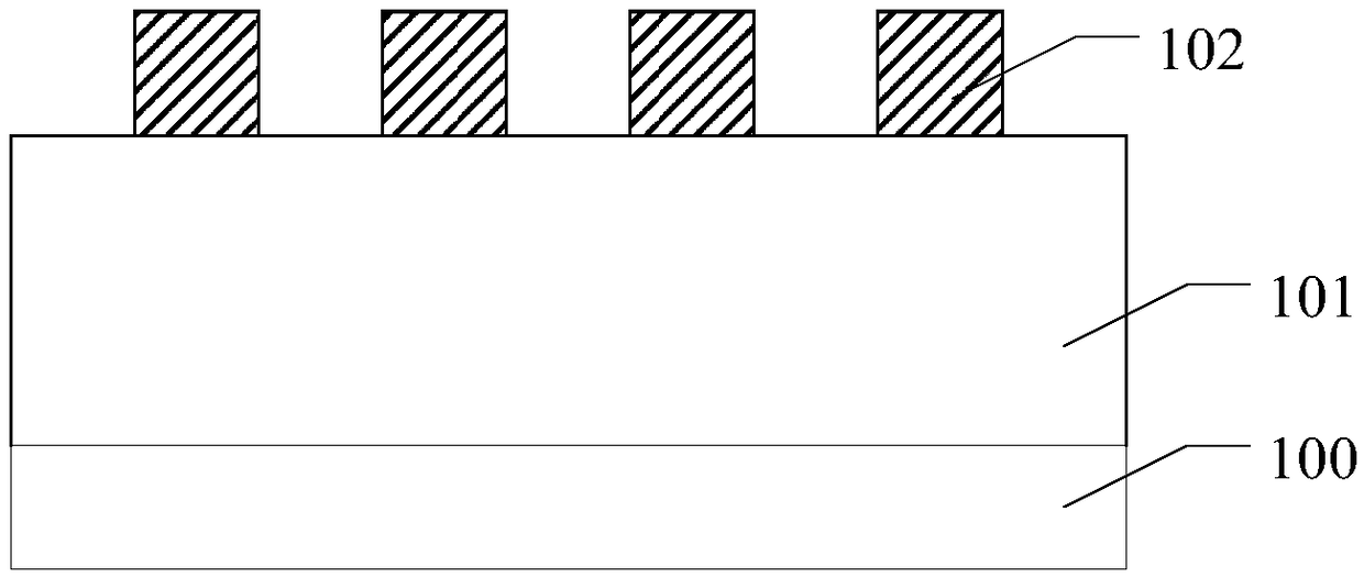
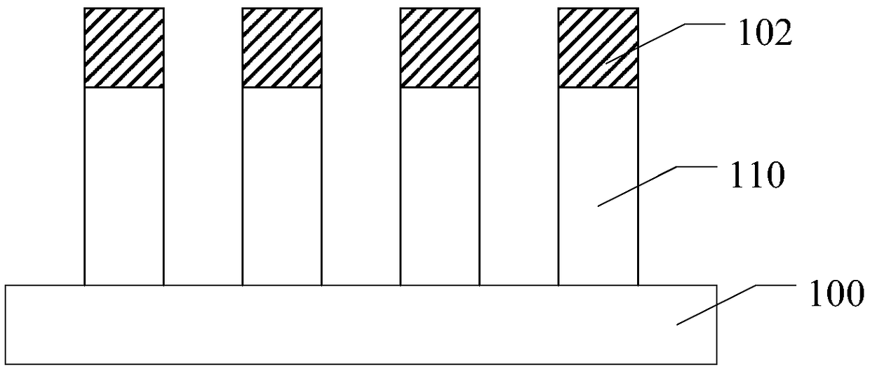
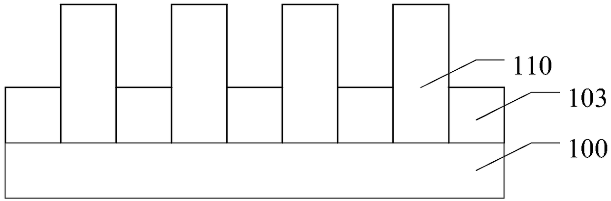
[0034] Figure 1 to Figure 3 It is a schematic cross-sectional structure diagram of the formation process of a semiconductor structure.

[0035] Please refer to figure 1 , providing a substrate 100 with a semiconductor film 101 thereon and a patterned layer 102 thereon, the patterned layer 102 defining the shape and position of the first fin.

[0036] Please refer to figure 2 , using the patterned layer 102 as a mask to etch the semiconductor film 101 (eg figure 1 shown) until the surface of the substrate 100 ...


PUM


Abstract

The invention provides a fin transistor and a formation method thereof. The formation method comprises the steps of providing a substrate, wherein the substrate is provided with a initial first fin portion and an initial isolation layer covering the side wall of the initial first fin portion; etching the initial first fin portion by taking the initial isolation layer as a mask, and forming a firstgroove in the initial isolation layer; and forming a first fin portion in the first groove, wherein the thermal conductivity coefficient of a material of the first fin portion is greater than the heat conductivity coefficient of a material of the substrate. The formation method effectively improves the heat transfer between the isolation layer and the substrate, improves a self-heating effect ofthe transistor and improves the electrical performance of a semiconductor device.

Description

technical field [0001] The present invention relates to the technical field of semiconductor manufacturing, and in particular, to a fin transistor and a method for forming the same. Background technique [0002] With the rapid development of semiconductor manufacturing technology, semiconductor devices are developing towards higher component density and higher integration. As the most basic semiconductor device, transistors are being widely used at present. Therefore, with the improvement of the component density and integration of semiconductor devices, the gate size of planar transistors is getting shorter and shorter, and the traditional planar transistors control the channel current. The ability becomes weak, resulting in a short channel effect, resulting in leakage current, which ultimately affects the electrical performance of the semiconductor device. [0003] In order to overcome the short channel effect of the transistor and suppress the leakage current, the prior ...

Claims


Application Information

Patent Timeline
IPC IPC(8): H01L29/06H01L21/336H01L29/78
CPCH01L29/0638H01L29/66795H01L29/785H01L21/76224H01L29/6681H01L21/823431H01L29/0642
Inventor 周飞
Owner SEMICON MFG INT (SHANGHAI) CORP
Why Eureka
Try Eureka