Fin field effect transistor and method of forming the same

A technology of fin field effect transistors and fins, which is applied to semiconductor devices, electrical components, circuits, etc., can solve problems affecting the electrical performance of FinFET devices, achieve the effect of improving self-heating effects and improving electrical performance

Active Publication Date: 2021-07-13
SEMICON MFG INT (SHANGHAI) CORP +1
View PDF0 Cites 0 Cited by
  • Summary
  • Abstract
  • Description
  • Claims
  • Application Information

AI Technical Summary

Problems solved by technology

However, when FinFET devices work, serious self-heating effects will occur, which will affect the electrical performance of FinFET devices

Method used


Image

  • Fin field effect transistor and method of forming the same
  • Fin field effect transistor and method of forming the same
  • Fin field effect transistor and method of forming the same

Examples


Embodiment Construction

[0034] The electrical performance of the fin field effect transistor formed according to the background technology needs to be improved.

[0035] The reason why the electrical performance of the FinFET needs to be improved is analyzed in conjunction with a FinFET.

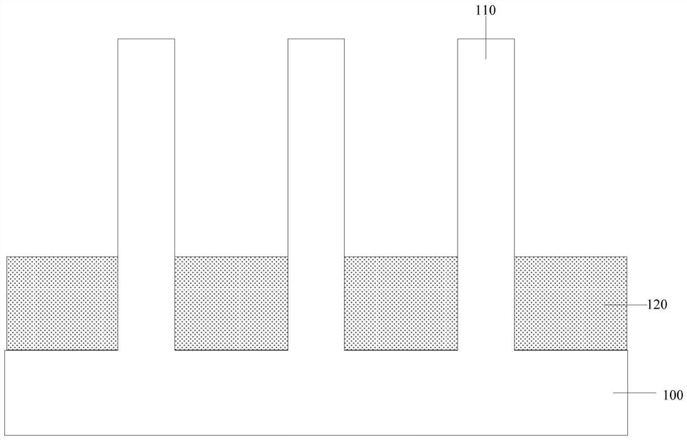
[0036] refer to figure 1 , figure 1 It is a schematic cross-sectional structure diagram of a fin field effect transistor, which includes: a substrate 100 ; and a plurality of fins 110 protruding from the substrate 100 . The isolation structure 120 is located on the substrate 100 exposed by the fin 110 , the isolation structure 120 covers part of the sidewall surface of the fin 110 , and the top of the isolation structure 120 is lower than the top of the fin 110 . across the gate structure (not shown) on the fin portion 110 .

[0037] When the above-mentioned FinFET is in operation, there will be a problem of self-heating effect, thereby reducing the electrical performance of the FinFET.

[0038]After analysis, ...


PUM

PropertyMeasurementUnit
thicknessaaaaaaaaaa
thicknessaaaaaaaaaa

Abstract

The present invention provides a Fin Field Effect Transistor and a method for forming the Fin Field Effect Transistor. The method for forming the Fin Field Effect Transistor includes: providing a semiconductor substrate with a plurality of discrete fins on the semiconductor substrate; A protective layer is formed on the semiconductor substrate between the fins and the bottom sidewall of the fin, the fin with the protective layer is the first region of the fin, and the fin without the protective layer is the second region of the fin; After the protective layer is formed, an initial isolation layer is formed on the protective layer and the fins; annealing is performed on the initial isolation layer in an oxygen-containing atmosphere to convert the initial isolation layer into an isolation layer, and the During the annealing process, the second region of the fin is oxidized to form an oxide layer on the sidewall of the second region of the fin; part of the thickness of the isolation layer is removed, and the oxide layer exposed by the remaining isolation layer is removed. The electrical performance of the fin field effect transistor formed by the invention is improved.

Description

technical field [0001] The invention relates to the technical field of semiconductor manufacturing, in particular to a fin field effect transistor and a forming method thereof. Background technique [0002] With the rapid development of semiconductor technology, the feature size of semiconductor devices is constantly shrinking, which makes the integration of integrated circuits higher and higher, which also puts forward higher requirements for the performance of devices. [0003] Currently, as the size of Metal-Oxide Semiconductor Field Effect Transistors (MOSFETs) continues to decrease. In order to adapt to the reduction of process nodes, the channel length of MOSFET field effect transistors can only be continuously shortened. The shortening of the channel length has the advantages of increasing the die density of the chip and increasing the switching speed of the MOSFET field effect tube. [0004] However, as the channel length of the device is shortened, the distance be...

Claims


Application Information

Patent Timeline
Patent Type & Authority Patents(China)
IPC IPC(8): H01L21/336H01L29/10H01L29/78
CPCH01L29/1033H01L29/66795H01L29/785
Inventor 周飞
Owner SEMICON MFG INT (SHANGHAI) CORP
Why Eureka
Try Eureka