Multi-chip package interconnection structure and multi-chip package interconnection method

A technology of multi-chip packaging and interconnection structure, applied in the field of electronics, can solve the problems of difficult to verify the reliability effectively, complicated manufacturing process, short interconnection length, etc. Effect

Pending Publication Date: 2019-02-12
中国科学院苏州纳米技术与纳米仿生研究所南昌研究院
View PDF8 Cites 6 Cited by
  • Summary
  • Abstract
  • Description
  • Claims
  • Application Information

AI Technical Summary

Problems solved by technology

The use of BGA solder ball interconnection has the advantages of good consistency, high integration density, and short interconnection length, but its manufacturing process is very complicated, resulting in high product costs, and it is difficult to effectively verify the reliability

Method used


Image

  • Multi-chip package interconnection structure and multi-chip package interconnection method
  • Multi-chip package interconnection structure and multi-chip package interconnection method
  • Multi-chip package interconnection structure and multi-chip package interconnection method

Examples


Embodiment Construction

[0020] In view of the deficiencies in the prior art, the inventor of this case was able to propose the technical solution of the present invention after long-term research and extensive practice. The technical solution, its implementation process and principle will be further explained as follows.

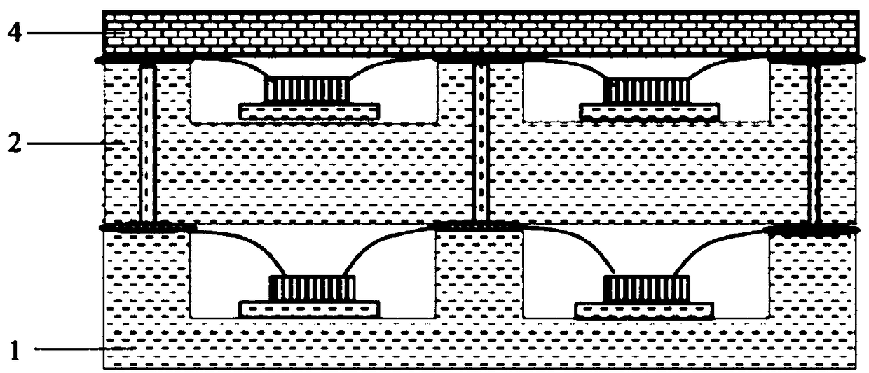
[0021] An embodiment of the present invention provides a multi-chip packaging and interconnection structure, including:

[0022] a first substrate and a second substrate arranged in layers;

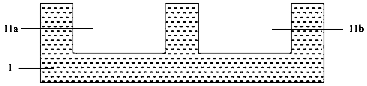
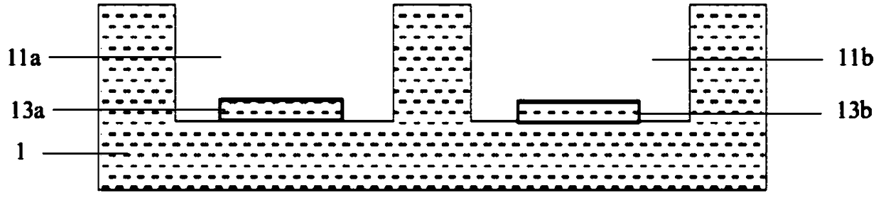
[0023] A plurality of first cavities are provided on the first substrate, a plurality of first chips are provided in the first cavities, a first pad is provided on the upper surface of the first substrate, and the first pad is electrically connected to the first chip;

[0024] A plurality of second cavities are provided on the second substrate, a plurality of second chips are provided in the second cavities, a second pad is provided on the upper surface of the second substrate, and the second...


PUM


Abstract

The invention discloses a multi-chip package interconnection structure, which comprises a first substrate and a second substrate which are superposed, wherein a plurality of first cavities are arranged on the first substrate; a plurality of first chips are arranged in the first cavities; the first surface of the first substrate is provided with a first pad; the first pad is electrically connectedto the first chips; a plurality of second cavities are formed in the second substrate; a plurality of second chips are arranged in the second cavities; the upper surface of the second substrate is provided with a second pad; the second pad is electrically connected to the second chips; the first pad and the second pad are electrically connected by a conductive medium penetrating the second substrate. The multi-chip package interconnection structure disclosed by the invention adopts a direct soldering method to realize the vertical interconnection of the substrates, so that multi-chip package is high in integration degree, good in reliability, simple in process and low in cost; microwave radio frequency signal insertion loss does not exceed 0.5 dB, which can solve the problem of high-density vertical interconnection of the substrates; and the multi-chip package interconnection structure is widely used in a multi-chip package system of a radio frequency microwave circuit.

Description

technical field [0001] The invention relates to the field of electronic technology, in particular to a multi-chip package interconnection structure and a multi-chip package interconnection method. Background technique [0002] With the rapid development of communication technology, VLSI technology, new electronic material technology and packaging and interconnection technology, modern military and civilian electronic equipment is developing in the direction of miniaturization, light weight, high reliability, multi-function and low cost. System-level three-dimensional packaging technology can contain multiple functions such as digital, analog, and radio frequency in a single package, which greatly reduces the volume and weight of the system. [0003] The key technology of 3D system-in-package lies in how to realize the vertical interconnection of the upper and lower layers of planar circuits. Vertical interconnection refers to the interconnection between signal layers, power...

Claims


Application Information

Patent Timeline
Patent Type & Authority Applications(China)
IPC IPC(8): H01L23/538H01L21/768
CPCH01L23/5384H01L23/5386H01L21/76897
Inventor 范亚明朱璞成
Owner 中国科学院苏州纳米技术与纳米仿生研究所南昌研究院
Why Eureka
Try Eureka