Chamfering processing equipment for full-automatic silicon wafer and processing technic thereof

A kind of processing equipment, fully automatic technology, applied in the direction of metal processing equipment, grinding/polishing equipment, manufacturing tools, etc., can solve the problems of time-consuming and labor-intensive, low work efficiency, etc., to save human resources, improve work efficiency, save self-adjustment The effect of the heart step

Pending Publication Date: 2019-02-15
浙江中晶新材料研究有限公司
View PDF1 Cites 2 Cited by
  • Summary
  • Abstract
  • Description
  • Claims
  • Application Information

AI Technical Summary

Problems solved by technology

[0005] However, the above-mentioned patents have not fully realized the full automation of the chamfering of single crystal silicon wafers. The chamfering of silicon wafers requires manual placement of silicon wafers on the processing table, which still requires manual operation, which is time-consuming and laborious, and there is only one Chamfering station, low work efficiency

Method used


Image

  • Chamfering processing equipment for full-automatic silicon wafer and processing technic thereof
  • Chamfering processing equipment for full-automatic silicon wafer and processing technic thereof
  • Chamfering processing equipment for full-automatic silicon wafer and processing technic thereof

Examples


Embodiment 1

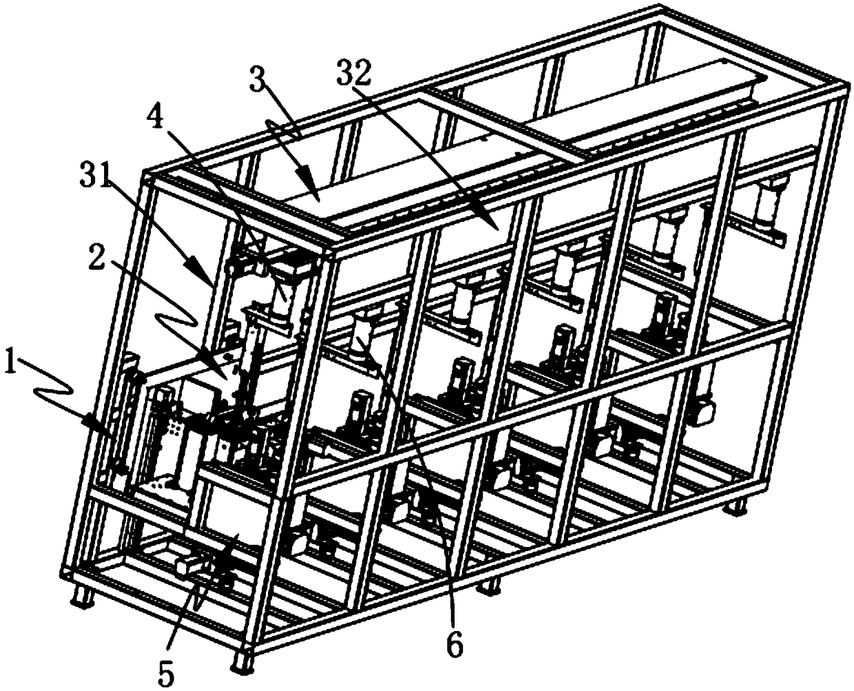
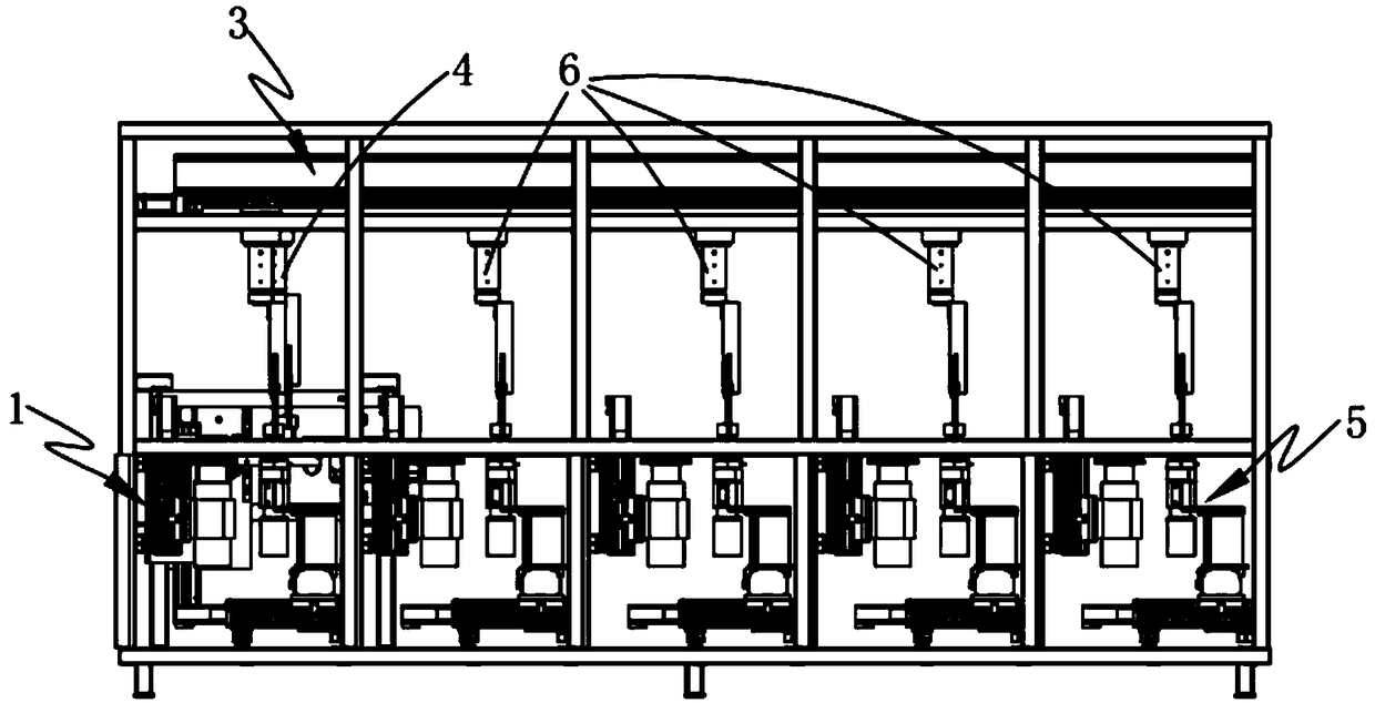
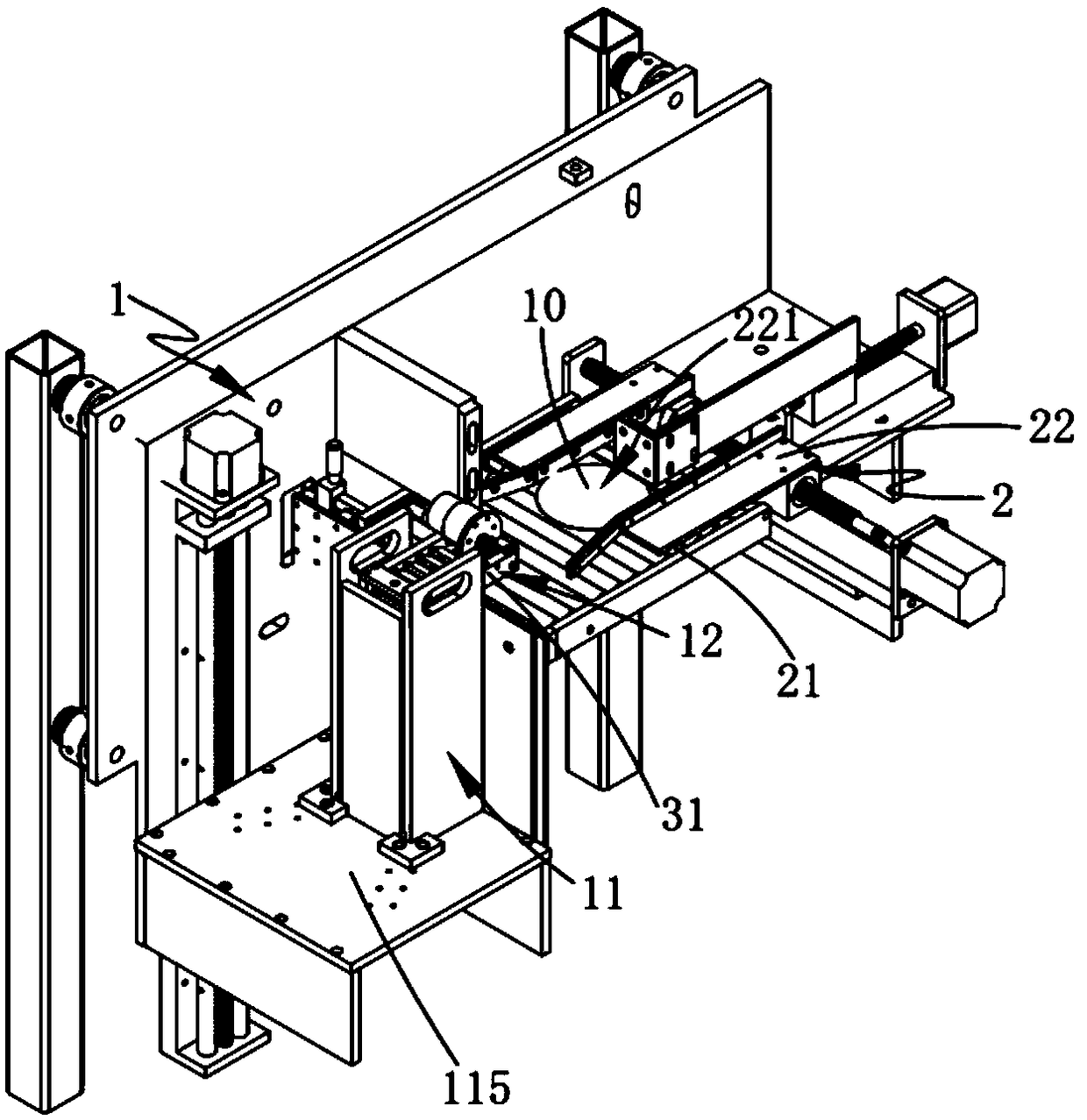
[0107] Such as figure 1 , figure 2 , image 3 and Figure 4 As shown, a fully automatic silicon wafer chamfering processing equipment includes:

[0108] frame;

[0109] Loading self-positioning unit I, the loading self-positioning unit I is installed at one end inside the frame, which includes:

[0110] Slice feeding device 1, which includes a feed lifting mechanism 11 for driving a cassette 118 with a number of silicon wafers 10 stacked inside to move upwards, and a slice loading mechanism 11 arranged on the rear side of the feed lifting mechanism 11. Institution 12; and

[0111] Transmission self-centering device 2, said transmission self-centering device 2 is arranged on the rear side of said piece-feeding device 1 and vertically arranged with said piece-feeding device 1, said transmission self-centering device 2 includes a transmission mechanism 21 And self-centering mechanism 22, the silicon chip 10 that is positioned at the top of sheet box 118 is automatically tr...


PUM


Abstract

The invention provides chamfering processing equipment for a full-automatic silicon wafer and a processing technic thereof; the full-automatic processing equipment for silicon wafer chamfering can realize single slicing and self-centering of piled silicon wafers by a slicing loading device and a transmission self-centering device; afterwards, the silicon wafers finishing the self-centering are grabbed by a grabbing device and the wafers placed on a chamfering device are realized under the movement of a silicon wafer transferring device; after the chamfering of the silicon wafer is realized onthe chamfering device, an automatic taking device can collect the silicon wafer in a silicon wafer collection box after taking the wafers; a processing method of one transferring mechanism matching with a plurality of sets of chamfering equipment is realized; human resource is saved; the technical problem that the chamfering equipment does not realize complete full automatic and has low working efficiency is solved; the processing technic for the full-automatic silicon wafer realizes quick single slicing and self-centering of the silicon wafer by using a silicon wafer slicing process and a silicon wafer locating process; and the silicon wafer can be transported to a plurality sets of chamfering equipment to conduct chamfering processing by using the silicon wafer transportation and siliconwafer placing.

Description

technical field [0001] The invention relates to the technical field of monocrystalline silicon wafer production, in particular to a fully automatic silicon wafer chamfering processing equipment and a processing technology thereof. Background technique [0002] As a good conductive material, monocrystalline silicon wafers can be widely used in technical fields such as semiconductors and solar cells. In the later stages of the processing of single crystal silicon wafers, steps such as chamfering, grinding, corrosion, polishing and cleaning are generally required. Among them, chamfering refers to trimming the sharp edges of the cut wafers into circular arcs to prevent wafer edge cracking and lattice defects. , so it is a very important process step. [0003] However, the chamfering machine for monocrystalline silicon wafers in the prior art is more complicated to operate, generally only one workpiece can be processed at a time, the workpiece needs to be clamped frequently, and...

Claims


Application Information

Patent Timeline
IPC IPC(8): B24B9/06B24B27/00B24B41/00B24B49/00
CPCB24B9/065B24B27/0023B24B41/005B24B49/00Y02P70/50
Inventor 万喜增严云黄笑容郑六奎
Owner 浙江中晶新材料研究有限公司
Why Eureka
Try Eureka