A kind of pcb preparation method and pcb thereof

A core board and board material technology, applied in multilayer circuit manufacturing, printed circuit manufacturing, simultaneous processing of multiple printed circuits, etc., can solve problems such as insufficient reliability of PCB, uneven pattern distribution, inconsistent shrinkage, etc., to improve the degree of curing and polymer cross-linking firmness, good curing effect, uniform heating and sufficient effect

Active Publication Date: 2020-02-28
DONGGUAN SHENGYI ELECTRONICS
View PDF8 Cites 0 Cited by
  • Summary
  • Abstract
  • Description
  • Claims
  • Application Information

AI Technical Summary

Problems solved by technology

Due to the expansion and contraction of film size, punching precision, material of riveting process, operation, equipment precision and other factors, the reliability of the produced PCB is low.
[0003] In addition, the PCB is directly exposed and etched by CCL. Due to the removal of part of the copper layer by etching, the internal stress of the PCB is released. Moreover, due to the uneven distribution of the graphics and the asymmetry on both sides, the PCB surface is warped after etching, and the coincidence is poor. The stress is released again in the combined state, resulting in inconsistent shrinkage, the long and short sides are non-rectangular, and become a twisted trapezoid, which leads to a sharp drop in the alignment between the core boards of each layer of the PCB, which in turn leads to a serious lack of reliability of the PCB

Method used


Image

  • A kind of pcb preparation method and pcb thereof
  • A kind of pcb preparation method and pcb thereof
  • A kind of pcb preparation method and pcb thereof

Examples


Embodiment Construction

[0021] Specific embodiments of the present invention will be described in detail below in conjunction with the accompanying drawings. It should be understood that the specific embodiments described here are only used to illustrate and explain the present invention, and are not intended to limit the present invention.

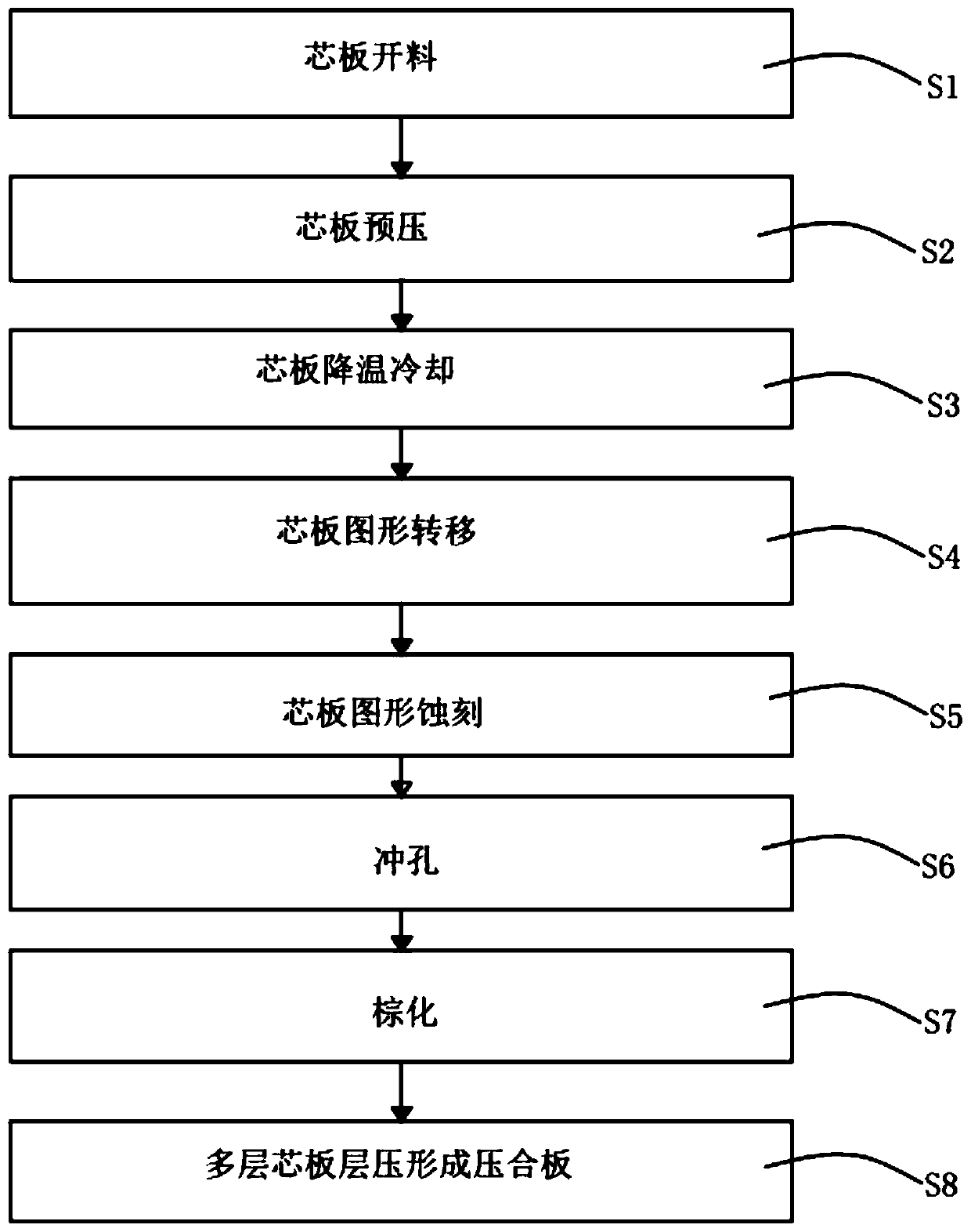
[0022] Such as figure 1 Shown, PCB preparation method of the present invention comprises the following steps:

[0023] S1: Core board cutting.

[0024] S2: Core plate pre-pressing; among them, the pre-pressing conditions are: the actual temperature of the plate is 5-10°C above the Tg point of the plate, the heating rate of the core plate is 2-4°C / min, the time is 60-90min, and the vacuum pressure is 350 ~450psi.

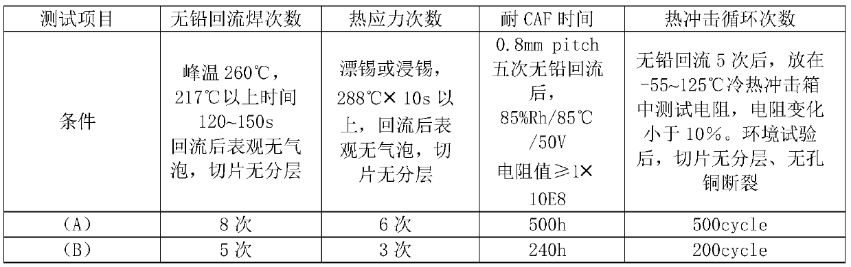
[0025] Taking a 28-layer board, 3.6mm thickness, 0.8mm pitch matrix 40╳40 BGA, and a PCB processed with a high Tg copper clad laminate as an example, the PCB (A) preloaded under the above preloading conditions is different from that under the non-th...


PUM


Abstract

The invention provides a PCB fabrication method and a PCB. The PCB fabrication method comprises the following steps of S1, opening a core board; S2, pre-pressing the core board; S3, cooling the core board; S4, transferring a pattern of the core board; S5, etching the pattern of the core board; S6, punching; S7, browning; and S8, laminating a multi-layer core board to form a lamination board. By the PCB fabrication method and the PCB, the reliability and the alignment of the PCB can be effectively improved.

Description

technical field [0001] The invention relates to the technical field of circuit board preparation, in particular to a PCB preparation method and the PCB. Background technique [0002] The existing PCB manufacturing process usually uses film exposure, PE-PUNCH punching, and riveting methods for exposure, punching, and superimposed typesetting. Due to the expansion and contraction of film size, punching precision, riveting process material, operation, equipment precision and other factors, the reliability of the produced PCB is low. [0003] In addition, the PCB is directly exposed and etched by CCL. Due to the removal of part of the copper layer by etching, the internal stress of the PCB is released. Moreover, due to the uneven distribution of the graphics and the asymmetry on both sides, the PCB surface is warped after etching, and the coincidence is poor. In the closed state, the stress is released again, resulting in inconsistent shrinkage, and the long and short sides are...

Claims


Application Information

Patent Timeline
Patent Type & Authority Patents(China)
IPC IPC(8): H05K1/02H05K3/00H05K3/46
CPCH05K1/0271H05K3/0097H05K3/4611H05K2203/068H05K2203/1476
Inventor 杜红兵傅宝林肖璐王小平
Owner DONGGUAN SHENGYI ELECTRONICS
Why Eureka
Try Eureka